
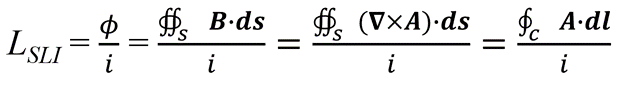
Inductance is defined as the ratio between the magnetic flux ϕ and the current i (see Equation (1a)).1 According to Ampère's law, current will generate a magnetic field H [A/m] and according to Equation (1b) the magnetic flux density B is determined by the environment permeability μ. (Bold letters indicate vector function.) Suppose the environment is homogeneous/isotropic satisfying Equation (1c), where the permeability constant μr is a scalar and not a tensor. In order to calculate the magnetic flux ϕ (see Equation (1d)), it is required to integrate the magnetic flux density components that are perpendicular (normal) to an area enclosed by a loop.
(1a) L = ϕ / i [Henry]
(1b) B = μ·H [V·s/m2] or [Tesla] or [Weber/m2]
(1c) μ = μ0·μr [Henry/m], μ0 is the vacuum permeability [4π·10-7 Henry/m]
(1d) ϕ = ∯ [B∙dS] [V·s] or [Weber]
The inductance which is presented and calculated in Equation (1a) is the Self-Loop Inductance (SLI) or, as we usually call it in short, “inductance.” The “loop” in the name comes from the fact that the area which the magnetic flux passes through is enclosed by a loop (the shape of the loop can be any enclosed shape). The “self” originates from the fact that the current flowing in the loop creates the magnetic flux inside the loop which defines its inductance. We shall mark this inductance as LSLI [Henry]. The SLI depends on the loop's geometry (shape, size) and the material surrounding it. If the current which flows in one loop creates a magnetic flux in another closed loop, then the Mutual-Loop Inductance (MLI) can be calculated.
Inductance is a major factor in Power Integrity (PI). The fact that the die (chip) consumes a transient current through the loop inductance of the PCB, the package and the die causes fluctuations in the die's power supply, which can cause problems related to timing (parallel interfaces), jitter (serial interfaces) ,increased noise on signals, duty cycle distortion (clock), pulse width distortion (data) ,reset, and chip life reduction. Therefore, among other things, the power integrity field deals with the proper design and layout of the PCB, the package, and the die, as well as with the optimal design of decoupling capacitance, in order to reduce inductance and resistance as much as possible.
For example, let’s take a 0.8 V power domain that is connected from the balls, through the package substrate, to the die. For simplicity’s sake, in this example, the package does not include On-Package Decoupling (OPD) and the ideal voltage source is connected directly to the balls without a PCB. It is certainly possible and valid to extend this example to include these components. Figure 1a shows the electrical circuit, which includes the current consumed by the die (die demand current vs. time), the On-Die Capacitance (ODC), and its series resistance RODC, the equivalent resistance of the Re-Distribution Layer (RRDL), and the package Resistor-Inductor (R-L) lumped model. The components with the red background are components on the die, while the components with the blue background are package components. Figure 1b shows the ports’ connection used for the extraction of the package resistance and inductance. In this example, all the Power (PWR) bumps are in one group, all the Ground (GND) bumps are in another group, and the port is connected between them. The same is done with the port at the balls' side. When the ports are connected, the current created by the ports flows through the PWR path and returns through the GND path. In this case, the extracted resistance is the total resistance of the PWR path and the GND path in the package, and the extracted inductance is the package loop inductance, as the current flows in a loop generated by the PWR path and the GND path. Therefore, one should consider that the GND path in Figure 1a is not ideal (i.e with zero resistance and negligible contribution to inductance). In this form of port connection, it is impossible to know what part each path plays in the total resistance or inductance. Figure 1c shows the package impedance magnitude vs. frequency. As can be seen, RLoop_PKG = 0.47 mΩ and is the dominant at low frequencies. The inductance LSLI_PKG = 11.5 pH and it starts to become dominant at a frequency of ~10 MHz. The resistance and inductance values were obtained by a simulation, where port 2 was set as a short.2 RLoop_PKG was extracted at DC and LSLI_PKG was extracted at a frequency of 300 MHz to allow the inductance value to stabilize after the skin effect and before resonances began to develop in the package. The voltage measured at point VT2 (shown in Figure 1d) is the voltage difference between the PWR bumps and the GND bumps. The total voltage drop (VT1 – VT2) on the PWR path and the GND path together is shown in Figure 1e; however, it is impossible to know how much of this voltage drop is due to the PWR path and how much is due to the GND path. The inability to analyze the drop on the PWR path and the GND path separately is a major disadvantage of this method.
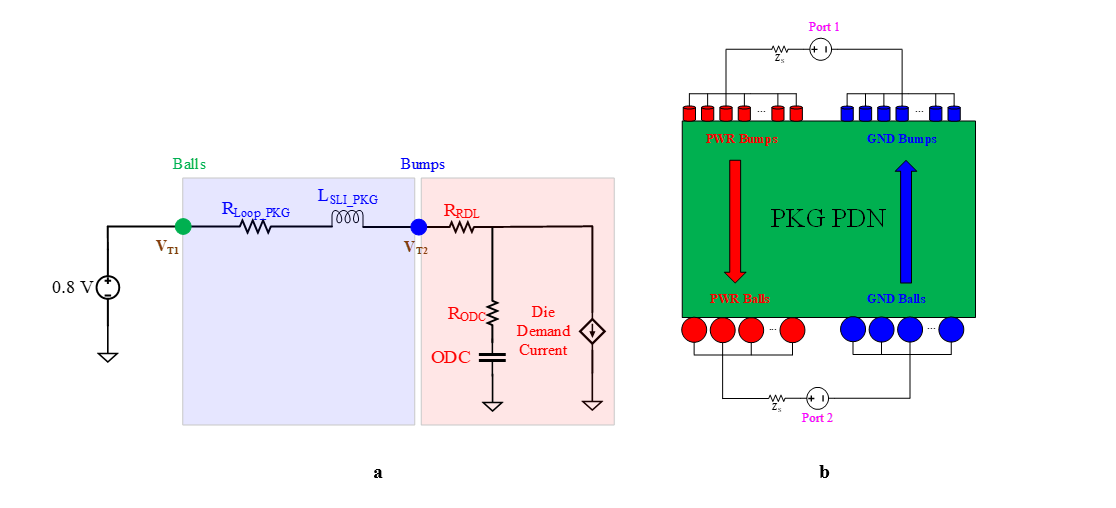
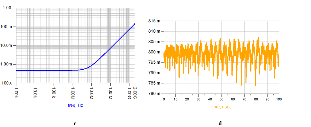
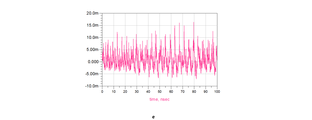
Figure 1. (a) The electrical circuit using package loop inductance and resistance. (b) Port connection for loop inductance and resistance extraction. (c) Package impedance magnitude vs. frequency. (d) VT2 - voltage difference between the PWR bumps and the GND bumps. (e) Total voltage drop on the PWR path and the GND path.
In many cases, this question is fundamental, therefore a different method is required to analyze the problem. This alternative method will be presented hereunder.
The overall loop resistance can be broken easily such that:
(2) RLoop_PKG = RPWR_PKG + RGND_PKG
When RPWR_PKG is the partial resistance between the PWR bumps and the PWR balls, and RGND_PKG is the partial resistance between the GND bumps and the GND balls. The “partial” in the name comes from the fact that this resistance is part of the overall loop resistance. But what about LSLI_PKG? How can LSLI_PKG be "broken"? To "break" LSLI_PKG, we must use a different method to calculate the SLI. In many electromagnetics problems, using auxiliary potential functions can simplify electric and magnetic fields calculations. Just as a scalar potential function is used in electrostatics to calculate the electric field, so a Vector Magnetic Potential A [V·s/m] can be used to calculate the magnetic field H. In many cases, it is easier first to calculate the vector magnetic potential A which is produced by a current, and then perform a simple derivative operation (curl) on A to calculate the magnetic flux density B. Dividing B by μ will yield the magnetic field H (see Equation (1b)).
Let's define the curl of A such that:
(3) B = ∇ × A
First, the definition in Equation (3) satisfies Maxwell equation ∇ · B = 0 (Gauss law for magnetism) since the divergence of a curl of a vector field is always identically zero (∇ · ∇ x A = 0). Now, if we take Equation (3) together with the other two Maxwell equations (Faraday's law and Ampere's law), apply Lorenz gauge, and organize the equations, we will get the relationship between the vector magnetic potential A and the source current density J [A/m2]:3
(4) (∇2 + k2 )A= -μJ
where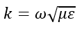
The equation in Equation (4) is the Vector Wave Equation. Several facts can be learned from Equation (4). Firstly, it can be concluded that A is produced by the current. We can also deduce that A has a direction parallel to the current that produced it, as well as that A is a wave and has wave properties. Lastly, it can be concluded that A goes to zero at infinity.
To break the SLI in Equation (1a), we shall use the magnetic flux definition in Equation (1d), the magnetic flux density definition in Equation (3) and Stokes' theorem:
(5)
The meaning of Equation (5) is that the magnetic flux ϕ can be traditionally calculated by integrating the magnetic flux density components that are perpendicular (normal) to the loop area. Alternatively, it is possible to calculate the magnetic flux by integrating the vector magnetic potential components that are parallel (tangent) to contour c enclosing the loop area. Dividing the magnetic flux by the current will yield the SLI.
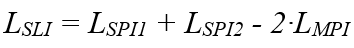
Now, to demonstrate how to break the loop inductance using the vector magnetic potential, we will bring a simple example of a loop containing two segments that contribute to the SLI (Figure 2). In Figure 2a, the current i1 flows in the first segment, which is on curve c1, creating the vector magnetic potential A1; the current i2 flows in the second segment, which is on curve c2, creating the vector magnetic potential A2. In this example, i1 = i2 = i. We will use the property of line integral on Equation (5) so the integration along contour c can be broken into two integrations, one on curve c1 and the other on curve c2 (see Equation (6)).
(6)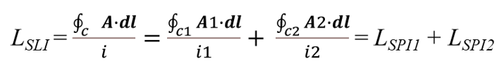
From Equation (6), it can be defined that the integration of the vector magnetic potential components that are parallel to the curve, divided by the current flowing in the same curve, is the Self-Partial Inductance (SPI). We shall mark it as LSPI [Henry]. Also, it can be seen in Equation (6) that the SLI is the sum of the SPI components in the loop (see Figure 2b). The “self” in the name comes from the fact that the vector magnetic potential A in a particular segment produced by the current flowing in that segment, and the “partial” comes from the fact that this inductance is part of the overall loop inductance. In other words, partial inductance is a way of breaking the overall loop inductance into its components. Equation 6 would have remained the same, had it not been for the mutual inductance. That is, A1 produced by i1 exists in the whole space including on curve c2, and A2 which produced by i2 also exists on curve c1 (see Figure 2c). Hence, they both also contribute to the overall loop inductance and should be added to Equation 6. Accordingly, when a vector magnetic potential in a particular segment produced by a current flowing in another segment, the Mutual-Partial Inductance (MPI) can be defined (Equations (7.1), (7.2)). We shall mark it as LMPI [Henry]. The “mutual” in the name can be attributed to the fact that A in a particular segment produced by a current flowing in another segment; the “partial” refers the fact that this inductance also contributes to the overall loop inductance, and is therefore part of it (see Figure 2d).
(7.1) 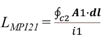
(7.2) 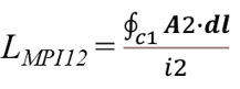
It would be advisable to note that A1 and c2 in Equation (7.1) run in opposite directions, therefore LMPI21 is negative. The same goes for LMPI12 in Equation (7.2). In addition, since the system is reciprocal, it can be determined that LMPI21 = LMPI12 = LMPI and the final expression for LSLI in the example is given in Equation (8).
(8)
From Equation (8), we learn that to break the SLI, we need to know both the SPI of each segment in the loop and the MPI between the segments.
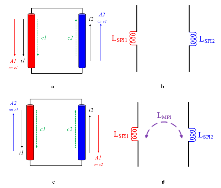 Figure 2. Expression of loop inductance with partial inductances: SPI (a, b) and MPI (c, d).
We shall now return to the circuit in Figure 1a and replace LSLI_PKG and RLoop_PKG with the partial inductances and resistances as shown in Figure 3a. In most cases, we will not calculate the partial inductance and resistance values analytically with paper and pencil, but we’ll use professional simulation tools for that. To extract the partial inductance and resistance values of each path separately, we need to connect the ports as shown in Figure 3b. By connecting the ports this way, the current flows once through the PWR path and once through the GND path and not through the loop created by the PWR path and the GND path. In this example, the PWR bumps are grouped together and so the GND bumps, but a separate port can be connected to each bump and then the results will be obtained separately for each bump. It would be right to do so in case the voltage is required for each bump separately. In the example, the following simulation results were obtained for the partial resistances (see Equation (9.1)) and the partial inductances (see Equation (9.2)).2
(9.1) RPWR_PKG = 0.32 mΩ, RGND_PKG = 0.19 mΩ
(9.2) LSPI_PWR_PKG = 17.7 pH, LSPI_GND_PKG = 14.4 pH, LMPI_PKG = 10.4 pH
Using Equation (2), it can be seen that RLoop_PKG of 0.47 mΩ is combined of 0.32 mΩ of the PWR path resistance and another 0.19 mΩ of the GND path resistance (a total of 0.51 mΩ compared to 0.47 mΩ in Figure 1c, a difference of 0.04 mΩ). If we calculate LSLI using Equation (8), we get 17.7 +14.4 -2·10.4 =11.3 pH, while the value in Figure 1c is 11.5 pH. Overall, a good match has been achieved between the resistance and inductance values obtained by both methods.
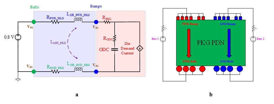
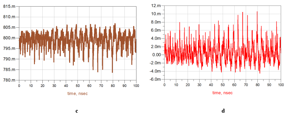
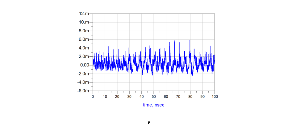
Figure 3. (a) The electrical circuit using partial inductances and resistances. (b) Port connection for partial inductance and resistance extraction. (c) Voltage difference between the PWR bumps and the GND bumps. (d) Voltage drop on the PWR path VP1-VP2 (e) voltage drop on the GND path VP4 - VP3.
The voltage difference between the PWR bumps and the GND bumps, calculated this time by the partial inductances and resistances (see Equations (9.1), (9.2)), is shown in Figure 3c. The result can be compared to that obtained by using loop inductance and resistance in Figure 1d. The difference between the results is less than ± 0.3 mV, so the correlation between the methods is very good. The advantage of using partial inductance and resistance is that it is now possible to know the voltage drop (DC+AC) on the PWR path, and the voltage drop (DC+AC) on the GND path separately. Figure 3d shows the voltage drop on the PWR path, which is the voltage difference between points P1 and P2 (VP1 – VP2), and Figure 3e shows the voltage drop on the GND path, which is the voltage difference between points P3 and P4 (VP4 - VP3). In the example, VP1=0.8 V and VP3 = 0V.
For example, Figure 1e shows that the maximum total voltage drop on the PWR path and the GND path together is 16.5 mV at 79.6 nS. Figure 3d and Figure 3e show how the 16.5 mV is divided between the PWR path and the GND path. There is a 10.7 mV drop on the PWR path, and another 5.8 mV drop on the GND path. In addition, Figure 1e shows that the minimal total voltage drop on the PWR path and the GND path together is -7 mV at 81.9 nS. Figure 3d and Figure 3e show that -4.5 mV of the voltage drop is on the PWR path, and another -2.5 mV drop is on the GND path. So, the maximum change between the PWR bumps and the GND bumps is 23.5 mV pk-pk around ~80 nS, where a 15.2 mV pk-pk drop is on the PWR path, and another 8.3 mV pk-pk drop is on the GND path.
Furthermore, if we average the voltage in Figure 1e, we get the DC drop on the PWR path and the GND path together (~0.36 mV). However, if we average the voltages in Figure 3d and Figure 3e, we can find the DC drop on each path separately. In that case, the DC drop on the PWR path is about 0.24 mV and the DC drop on the GND path is about 0.14 mV (a difference of 0.02 mV between the methods). Although the DC drop is negligible in this example, there may be examples where the DC drop will be significant, and it will be necessary to know what is the DC drop on each path separately. Of course, one may extend this analysis precisely the same way by adding the PCB with its partial inductances and resistances in order to get the voltage drop on the PWR path and the GND path from the voltage regulator module to the balls. It is also possible to add the decoupling capacitors on the package and on the PCB to the electrical circuit.
From a practical point of view, to get a good match in the values of the resistances (see Equation (2)) and inductances (see Equation (8)), it would be acceptable to use the same simulation tool and the same solver in both cases. In addition, as in any electromagnetic simulation, the boundary conditions may affect the simulation results.
REFERENCES
1. C.R. Paul, "Inductance," John Wiley & Sons, Inc. Publication, 2010.
2. "HyperLynx Fast 3D Solver," VX.2.8 Update 3, Mentor, A Siemens Business
3. S. V. Hum, "Radio and Microwave Wireless Systems," University of Toronto, Faculty of Applied Science and Engineering.