Digital interconnects are modeled as transmission lines defined by characteristic impedance and propagation constant. This article explains how transmission lines work and provides practical formulas for investigation of signal degradation due to absorption and reflections losses. Optimal characteristic impedance is defined for printed circuit board (PCB) and packaging interconnects as the impedance that minimizes the power absorbed by interconnects and terminators. It is shown that 50 Ω single-ended or 100 Ω differential may be not optimal if we need either longer reach or spend less energy per bit transmitted over interconnects.
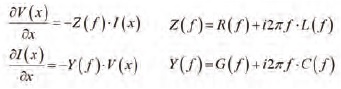
Where I is the current, V is voltage changing along the x-axis, f is frequency (Hz). Z(Ω/m) is complex impedance per unit length and Y (S/m) is complex admittance per unit length, R(Ω /m) and L (Hn/m) — are real frequency-dependent resistance and inductance per unit length, G (S/m) and C (F/m) — are real frequency-dependent conductance and capacitance per unit length. Z, Y, R, L, G, and C for N+1 conductor problem or N-mode transmission line are NxN matrices in general. They are 2×2 matrices for a three-conductor differential line for instance. The impedance and admittance per unit length are frequency-dependent, in general, and are completely defined by transmission line type and cross-section and usually computed either with a static or quasi-static 2D field solver or sometimes with 3D EM solvers. Note that the use of 3D solvers does not automatically guarantee higher accuracy.
A solution of the Telegrapher’s equation can be written as a superposition of two waves propagating in opposite directions as follows (can be easily verified by inspection):
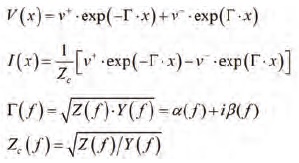
Where Zc is complex frequency-dependent characteristic impedance and gamma is complex propagation constant ( is the attenuation constant (Np/m) and beta is the phase constant (rad/m) defined as
  Lambda is the wavelength in the transmission line — phase changes by
  over that length, see more in the Appendix). Those are the modal parameters in general — the equations above are for a two-conductor line with one mode only. If we write the solution for the wave propagating only in one direction along the x-axis for instance (would be ideal for signal transmission):
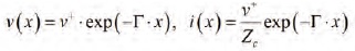
We can see that the characteristic impedance is just a ratio of the voltage and current of the wave propagating in one direction of transmission line v(x)/i(x)=Zc. It is impedance by dimension (Ω). It is pure resistance if line is lossless. The word “characteristic” is used because it does not depend on the position or length of transmission line segment (independent of x) — it “characterizes” it. It depends only on the type of transmission line and geometry of the cross-section. Note that for planar transmission lines, used for PCB and packaging interconnects, the definition of impedance is not unique and can be done in three ways — through voltage and current, current and power, and voltage and power, but they all close to the conventional “static” voltagecurrent definition if cross-section remains much smaller than the wavelength, which is usually good assumption for PCB and packaging interconnects.
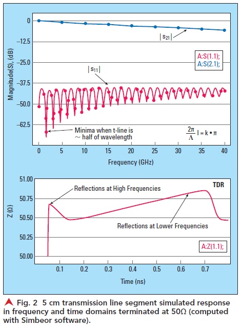
To investigate the reflections, the next step is to define the properties of a transmission line segment. The Telegrapher’s equations introduced in the previous section are incomplete without the “boundary conditions” or terminations. The most effective way to describe a segment is to use waves and scattering parameters (Sparameters). Here is a transmission line segment with length l connected to voltage sources with all variables, to define S-parameters:
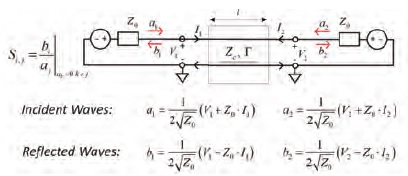
Where a1, a2 are the “incident waves,” and b1, b2 are the “reflected waves” with dimension sqrt (Wt). V1, V2 and I1, I2 are voltages and currents at the segment ports (pairs of terminals). Z0 is the termination or normalization impedance (same thing in this context). Waves in this definition are not actual waves in the transmission line, but rather variables formally defined through voltage and current. Using equations for voltage and current in the transmission line segment (superposition of two waves defined earlier) and Kirchhoff’s laws at the external terminals or by following more formal procedure from “S-parameters for Signal Integrity,”4 we can define S-parameters or S-matrix that relates the incident and reflected waves for such segment as follows:
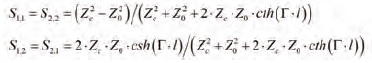
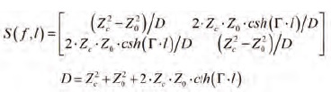 The reflection (S11 and S22) and transmission (S12 and S21) can be expressed separately as follows:
 Note that the transmission parameters include the effects of absorption and reflections — there are no approximations in these expressions. This is a universal definition of the reflection and transmission — it can be used for simple experiments with transmission line properties or as rigorous modelling of a segment. It depends on the definition of characteristic impedance and propagation constant used. The rest is pure trigonometry. You can start with a frequency-independent capacitance and inductance per unit length or use more complicated expressions for the characteristic impedance and propagation constant.5 For simple experiments, the propagation constant can be defined analytically with formulas or simply with phase delay or propagation velocity for ideal lines (see Appendix). This is a simple and important tool for all kinds of experiments in the frequency domain with real transmission lines. It includes all reflections in time domain (if model bandwidth is properly defined).1 Though, use of frequency domain response for time domain analysis is not as easy.4 Simbeor software is used here for all frequency and time domain analyses — it makes our investigation easier.
Now, what useful information can be derived from such a simple trigonometric model? Let’s begin from a very simple case of the termination or normalization impedance equal to the characteristic impedance Zo=Zc — the reflection parameter is zero in this case as we can see from the formula. The S-matrix in this case is simple and defined as follows (generalized modal S-parameters):
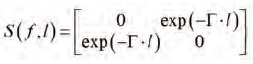
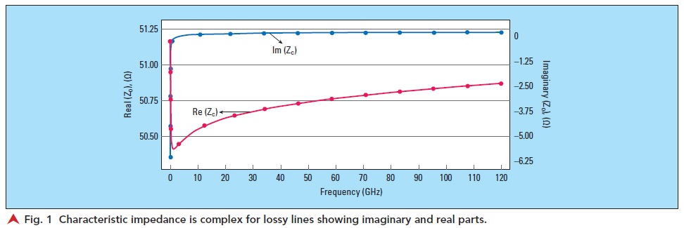
Only the transmission parameters and no reflections — this should be the Holy Grail of the interconnect design — the signal is travelling strictly in one direction. Though, the signal may still not get through because the transmission parameter depends on the absorption and dispersion in Gamma discussed earlier.2 Considering the zero-reflection condition, why do we not do it like that way? First, the characteristic impedance is complex for lossy lines — it has real and imaginary parts. The zero-reflection termination is not just a resistor — it should be frequency dependent. But this is not the showstopper— the real part of the characteristic impedance does not change much at the important frequencies and the imaginary part is much smaller than the real part, as can be seen in Figure 1 (typical PCB case).
So, at least theoretically, we should be able to get very close to the non-reflective case. Practically, there are more factors that do not allow this to happen — the manufacturing variations and discontinuities such as pads and viaholes are the most important ones.