If you routinely give attention to trace impedance but are not accustomed to thinking about via impedance, this article is for you. Or, if you are paying attention to via impedance yet are unsure what dimensions will yield the right impedance, this will help with that too. So, when should I use an 8 mil drill?
Why Should I Care?
Serial links can fail because of impedance mismatches, or discontinuities. In practice, discontinuities are causing more problems than loss. While loss degrades a signal somewhat predictably and can be compensated by equalization, discontinuities cause reflections that are much harder to tame. So, fix the discontinuities and you fix the signal. An example of a 400% eye improvement achieved by correcting via impedance is shown in the article, “Moving Higher Data Rate Serial Links into Production – Issues & Solutions;” a mere 1% of the interconnect.1 Another method to improve via impedance is shown in “New SI Techniques for Large System Performance Tuning,” and its resulting performance improvement measured in hardware.2
Although they are small, vias can significantly impact performance. This first became apparent when ¼ wavelength stubs crept into systems. A via stub left in a ¼ in. thick backplane can completely remove a 12 Gbps signal, per the approximation 3/12 (yes, just use 3 divided by Gbps and get inches).3 While stubs can be disastrous, via impedance mismatch is also increasingly problematic as data rates increase. But how can we better understand the impedance of vias?
Enter Via Modeling
A few decades ago, while my RF friends were busy with exotic 3D solutions of vias, we would place a 0.5 pF capacitor in our interconnect model at via locations and call it good. Over time, we learned that modeling vias as a transmission line is a better approach. Some tools implement fast via solvers4 that expand on the transmission line concept to deliver correlated accuracy, as described “Fast, efficient, and accurate: via models that correlate to 20 GHz.”5 Yet even if you don’t have access to a fast via solver, it is possible to gain an intuitive sense of via impedance, as described here. And if you want to try out a via solver, a link is provided at the end of this article.
Building Impedance Intuition
To build our intuition on what via dimensions will yield impedances we want, let’s begin with the more familiar differential trace shown in
Figure 1. Indeed, vias behave a bit like traces—albeit in the Z dimension.

Figure 1 shows stripline trace impedance versus width, spacing, and distance to ground planes (X-axis represents W=S=H1=H2 per the cross-section view). Interestingly, all dimensions yield impedances close to what we typically want, and minor adjustments are used to dial in the value more precisely. For example, increasing either or both H values moves the reference plane further away, making the trace more inductive, thus raising the impedance (Z=sqrt[L/C]). Widening the trace (W) makes the trace more capacitive, thus lowering its impedance. Visualize how these two changes impact impedance, because we are about to apply them to via structures.
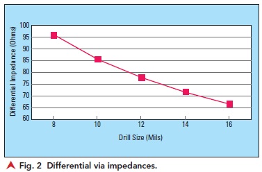
Figure 2 plots differential via impedance versus common drill sizes on the X-axis. Pad sizes are drill+10 mils and circular antipad sizes are drill+20 mils. Spacing is 1 mm as would be found under a BGA or near a connector. The first thing we notice is the range of impedances has increased more than 4× when compared to the range of trace impedances in
Figure 1. This wider range makes via impedance more challenging to control. Like traces, we can make changes to a via’s structure to adjust its impedance. For example, widening the antipads—or connecting them into an oval “racetrack” shape—moves the reference plane further away (like increasing trace H in Figure 1) making the via barrel more inductive thus raising its impedance. In contrast, increasing the drill size widens the barrel (like increasing trace W) making it more capacitive, hence lowering its impedance.
Again, the challenge with vias is the 4×+ impedance range compared to the narrower range associated with traces—seen clearly by comparing Figure 1 and Figure 2. As structural adjustments for traces and vias have similar dimensions, they also have similar effects on impedance—perhaps 5 Ω or 10 Ω in either direction. As such it becomes difficult to get 16 or even 12 mil vias close to 100 Ω because their “natural” (i.e., no structural modifications) impedances are ~70 Ω. Thus, it should become apparent why 8 mil drills are gaining in popularity in a world somewhat reluctant to move towards 85Ω impedance—which is the “natural” impedance of the more common 10 mil via.
Digging Deeper
You might be objecting to my generalizations because I did not state my dielectric constant (Dk). You’re right—it is 3.3. Dk proportionally raises capacitance and hence inversely affects impedance. As such, the first time I solved 10 mil vias with a Dk = 3.0, I found them closer to 100 Ω than expected. With common Dk values varying 50% (3.0 to 4.5), Dk is indeed an
important consideration. So, when using the differential impedances shown in Figure 2, if your Dk is higher than 3.3, your impedance values will be lower. Likewise, if your Dk is lower than 3.3, your impedances will be higher. For example, as Dk ranges from 3.0 to 3.6, the Figure 2 impedances change ± ~4 Ω.
We should also discuss differential trace and via spacing. As traces or vias get closer together they become more capacitive and hence impedance decreases. While the trace impedances shown in Figure 1 can be increased ~10 Ω by separating the traces, via impedances will decrease from those shown in Figure 2 as vias move closer together. However, due to their associated pads, via barrels cannot move closer together than ~20 mils, making it difficult to decrease impedance by more than ~5 Ω.
Also, be advised that as we pass 28 Gbps NRZ data rate, we need to stop thinking of vias as a single impedance, but instead as a structure whose impedance dips at the pads and rises in the barrel. At this data rate those elements are within the relevant feature size and, therefore, are modeled separately.6
Conclusion
As you start down the road of grappling with via impedances—and more tools and measurements become available for the same—the task will simplify, just as it did for traces. My goal has been to give you a reference point to make the task of implementing via impedances—thus removing via impedance discontinuities—less daunting. Want to try out automated solvers with your via dimensions? Download a free trial of Signal Integrity Toolbox which includes a Via Editor tool.7
*This article is an excerpt from Donald Telian’s new book “Signal Integrity, In Practice.” A Practical Handbook for Hardware, SI, FPGA, and Layout Engineers. Available at Amazon.
REFERENCES
1. D. Telian, S. Camerlo, K. Matta, et al. ,“Moving Higher Data Rate Serial Links into Production – Issues & Solutions,” DesignCon, 2014, page 4.
2. D. Telian, M. Steinberger, B. Katz, “New SI Techniques for Large System Performance Tuning,” DesignCon, 2016, page 21.
3. D. Telian, “Adapting Signal Integrity Tools and Techniques for 6 Gbps and Beyond,” SiGuys, CDNLive!, slides 1-33, 2007, slide 5.
4. D. Telian, S. Camerlo, M. Steinberger, et al., “Simulating Large Systems with Thousands of Serial Links,” DesignCon, 2012, page 4.
5. M. Steinberger, D. Telian, E. Brock, “Fast, Efficient and Accurate: via Models that Correlate to 20 GHz,” DesignCon, 2013.
6. D. Telian, “Which Discontinuities are Small Enough to Ignore?” Signal Integrity Journal RSS, April 2022, Figure 2.
Donald Telian is a Signal Integrity Consultant, the owner of SiGuys, and the author of the book “Signal Integrity, In Practice” now available at Amazon. He has worked in Signal Integrity for 40 years.
