
In earlier DDR systems, the clock, command, and address signals (here in referred to as C/A) were distributed to multiple DRAMs using a forked topology, in which these signals propagate to all the DRAMs in the system at approximately the same time. The propagation delays on the command and address lines (in such systems) introduced timing skew into the system, limiting the operating frequency of the bus and eventually impacting the performance of these memory systems.
The performance of a C/A bus is also limited by capacitive loading. Adding more memory devices to increase memory capacity on the module (DIMM) increases the capacitive loading of the C/A lines, thereby limiting the maximum signaling rate on the C/A line. For this reason, in large server designs (where a lot of memory is required, and therefore capacitive loading would be high), a Register IC is placed on each DIMM card. Signals enter the Register IC, and the C/A signals are then re-transmitted out to the individual DRAMs.
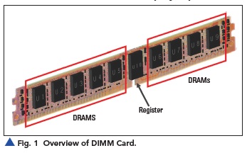
‘Fly-by’ command/address architectures presented here as ‘multi-drop’ channels improve signal integrity in memory systems by addressing the capacitive loading and the timing skew issues. In this article, we explore some features of this multi-drop fly-by command/address architecture implementation. To simplify things, we will base our exploration on a DIMM card that has a single register and multiple DRAM chips on the right and left of it (see Figure 1). Though the concepts explored here apply equally to system-level PCB designs as well.
Understanding Multi-Drop Fly-by Architecture
The fly-by architecture optimizes the topology of system transmission, is more tolerant of timing skews, and enables point-to-point signal lines with scalable capacity without compromising memory data rates. In this fly-by architecture, the clock, address, and command are transmitted source synchronously to the DRAMs. As shown in Figure 2, the clock signal propagates with the address and control information such that these signals arrive together at the interface of each DRAM. However, in this topology, the set of signals propagating on these lines arrives at each DRAM at a slightly different time.
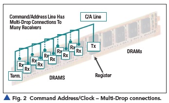
Since the arrival times of the signals at the DRAM interfaces are distributed in time, the time at which the signals encounter the input capacitance of each of the DRAMs is also distributed, thereby reducing the capacitive loading. The reduced capacitive loading enhances the signal integrity and enables higher data rate signaling.
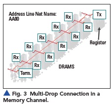
In Figure 3, we see a single address line signal net, named AA00 (as shown in Keysight ADS SIPro). This diagram clarifies the path the signal takes, such that the signal arrives at a different time at each of DRAM Rx interfaces. We will now analyze this selected signal net.
Analysis at Low Frequency
We first perform simple analytical calculation (pencil + paper) of the transmission coefficient [T(dB)] for such a multi-drop bus connection. We compare this analytical calculation result with the EM solver result at low frequency. To perform this analysis, we translate our network shown in Figure 3 into an equivalent circuit as shown in Figure 4(a).
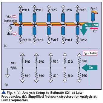
In this equivalent circuit, we have drawn an interface where the signal (incident wave) is launched from Port 1. Now, since we are analyzing this circuit at low frequency, the wavelength of the transmitted wave results in no amplitude and phase variation over the physical length. We, therefore, can treat the network as one lumped node (this will be Port 2). In this case S21 simplifies to become transmission coefficient [T(dB)].
Also, we need to understand another basic assumption made in this analysis: all port impedances (terminations) are to be considered 50 Ohms. This assumption is made in this analytical method to easily compare our result with the one from the EM solver (because the EM solver gives S-parameter value with a reference impedance of 50 Ohms). With this assumption, our equivalent circuit at low frequency results in a much-simplified network of eleven 50-Ohm impedances forming a parallel network as shown in Figure 4(b).
Now, we solve for the input impedance Zin and subsequently determine the S21 value at low frequency.
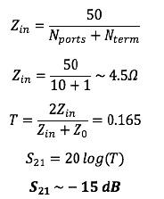
Now, we have determined the value of S21 at low frequency using the simple (pencil + paper) approach, and we expect -15 dB as the result from our simulator/solver as well. This is the result you would expect from an S-parameter extraction provided by an EM simulator. Figure 5 shows the result of insertion loss at low frequencies for all 10 different ports obtained from an EM simulator, in this instance Keysight ADS SIPro. At low frequency, the EM Solver has also produced the same result of -15 dB (highlighted with red box) which shows that all ports are equivalent and thereby confirms our initial analytical assumption that all ports act as a single node at low frequency.
This agreement between the analytical and simulation result builds confidence in the use of the given solver. Let’s now analyze this structure at high frequencies.

Analysis at High Frequency
At high frequency, the wavelength of the incident signal results in a variation of amplitude and voltage along the length of the structure. This results in making the analytical (pencil + paper) approach not feasible for high-frequency analysis. We rely instead on a computational EM solver to include the distributed transmission line effects and losses in our analysis to determine the transmission coefficient [T(dB)] for all the ports. Figure 6 shows the response of insertion loss of all 10 ports for frequencies up to 10 GHz frequency.
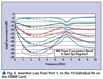
The different insertion loss results in Figure 6 are not the usual responses that we are accustomed to observe in high-speed digital channels. Usually we expect the response of insertion loss (S21) to be starting at 0 dB at low frequency and monotonically dropping off for a single point-to-point high-speed digital channel. Since we are not observing the usual response (and assuming we are new to the world of multi-drop memory system design), we need to recalibrate our understanding for proper analysis of a multi-drop topology.
Recalibrating Our Understanding
In this setup, we do not have a single channel with a distinct input and output port to have a usual response of insertion loss. In the previous section of this article, we clearly see that the response at low frequency is -15 dB due to the multi-drop structure. This value of insertion loss at low frequency depends on the number of DRAMs connected to the bus (in the above case it resulted in insertion loss of -15 dB). This same structure results in two lines (related to ports 10,11; far end side) to have insertion loss of about -50 dB at around 3 GHz as seen in Figure 6. We need to understand that a multi-drop topology is inherently not impedance controlled; there are mismatches at every stub along the line resulting in the insertion loss profile shown.
The design flow for memory system analysis will help us relate the EM extracted S-parameter dataset and its use in determining if we will get an open eye diagram for a specific DRAM. We get the S-parameter results from an EM solver which characterizes the physical nature of the multi-drop topology. We then use the DDR bus simulator in Keysight ADS along with this EM extracted S-parameter dataset (PCB information), the controller (Tx) models and DRAMs (Rx) models to analyze the eye opening. These DRAM modules act as a high impedance (capacitive loads) for the multi-drop topology. Due to high impedance termination of DRAMs and relatively low characteristic impedance of the multi-drop channel, there are multiple reflections on this multi-drop channel.
The length and spacing of the stub loads relative to the frequency of the exciting signal determine if these reflections will interfere constructively or destructively. As memory system designers, it is important for us to optimize the length and spacing of the stub loads such that we get constructive interference and therefore an open eye diagram. In a multi-drop topology, the impedance mismatch and reflections are used to the benefit of the designer to obtain an open eye diagram.
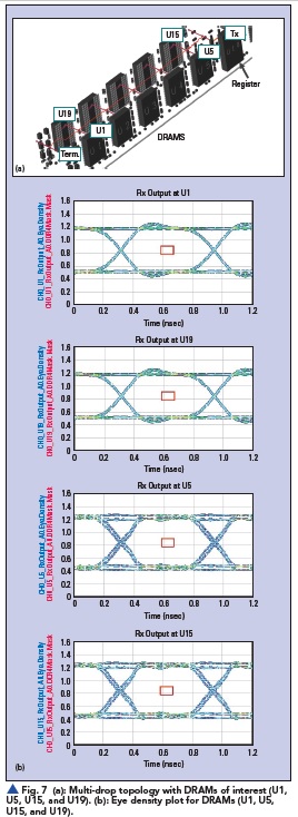
If we try to understand the significance of optimized length and spacing of the stub loads relative to the frequency of the exciting signal, we arrive at the conclusion that the response at each of the ports will be unique, resulting in a different eye diagram at each port due to the spatial variation of the interference and the resulting amplitude and phase variation along the line. To illustrate this, consider the structure shown in Figure 7(a). In this diagram, we have U10 as the controller (Tx), and we are interested to observe the eye diagram for DRAM (Rx) - U1, U5, U15, and U19.
Now, we have plots for four eye diagrams in Figure 7(b) showing that if DRAMs are placed at the same point spatially away from the controller, they will result in a similar eye diagram. This is observed by comparing the eye diagrams for U1 and U19 or U5 and U15. For DRAMs placed spatially at different locations we get different eye diagrams. This is observed when we compare eye diagrams for U1 and U5.
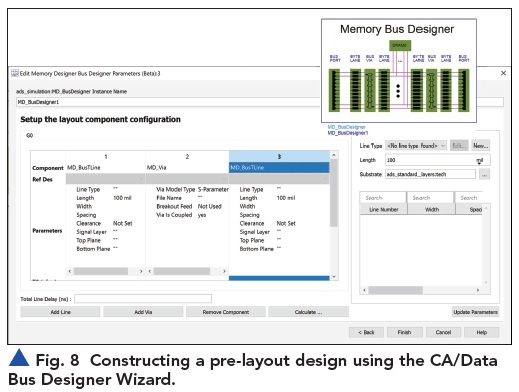
With this new understanding of how constructive interference plays an important role in opening of the eye, we need to layout the signal net with optimum length and spacing of the stub loads relative to the frequency of the exciting signal. The required analysis to determine the net layout dimensions, for a specific PCB stack-up, on specific layers, can be obtained in the pre-layout phase of the design flow. For this purpose, we used the CA/Data Bus Designer Wizard in Keysight’s ADS Memory Designer. Figure 8 shows the construction of a pre-layout design which can cascade parameterized transmission lines and via structures to form the expected layout geometry for analysis.
In summary, when evaluating the performance of a multi-drop bus, the S-parameter results are certainly very different to what would be expected of a typical point-to-point high-speed channel. This is where a good pre-layout representation of the design is critical to recalibrate our expectations and allow us to validate how the optimal design should behave. Ideally all new designs should begin with a pre-layout model representation first before progressing into physical layout. However even if an existing layout artwork has been leveraged into a new design, then using a wizard to quickly build the pre-layout representation can aid with troubleshooting and further optimization. Fly-by trace routing would be optimized to (1) reduce skew between the C/A signals and the clock, at each of the multi-drop Rx ports, (2) reduce impedance mismatches in the path, and (3) maintain optimum length and spacing of the stub loads relative to the frequency of the exciting signal that provides constructive interference at each Rx. These design elements are necessary for great signal integrity at the higher data rates required of DDR4 and DDR5.
Published in the SIJ 2022 Print Issue, Technical Feature: Page 32.