
New electronic applications, such as electric vehicles, 48 V telecom/data centers, and 240 W USB power delivery, demand higher voltage power supplies. These higher voltage power rails are no different from traditional 3.3 V, 5 V, and/or 12 V rails. Having a noisy power supply significantly degrades the performance of the load circuit, hence the need for very low output ripple and noise voltage. Since many of these application circuits convert power supply noise into output signal noise of amplitude or phase, it is most useful to measure the power supply noise using a spectral noise density plot.
In this power-electronics article, we focus on noise measurement of 48 V range voltage regulators (VRs), up to a maximum of 65 V. We propose a noise measurement setup and examine this method.
Regulator Noise Impact
As an example, we know that an RF power amplifier (PA) modulates its DC bias noise on the RF output. This modulation is known as power supply modulation ratio (PSMR), and the measurement of DC bias supply spectrum is the input of this ratio characteristic. Figure 1 illustrates the concept of PSMR, the input and output signals.

The base plot, in blue, is an output signal spectrum of an RF PA, where we superimpose a DC bias VR noise curve obtained by the method of this article, in light red color.
In this example, we use a switch mode power supply (SMPS) as the VR, so we can clearly see some spurs from the switching operation and its harmonics. This VR is operating at 500 kHz, and 0.5 MHz spurs are the main switching noise in both the light red and blue plots. Then, we observe second and third harmonics at 1 MHz and 1.5 MHz.
Measurement Challenges
It is common knowledge how to measure 3.3 V and 5 V regulator output noise. We just hook up the designated regulator output to a spectrum analyzer and the job is done.
The input ports of most spectrum analyzers are terminated in 50Ω. A 5 V regulator connection, for example, results in 100 mA/0.5 W of current flow. Usually, an input DC voltage maximum limit is set to 5 V for a 50Ω terminated port. An input port can be damaged when directly connecting a 50 V supply if it causes a 1 A/50 W current flow.
Some analyzers and pre-amplifiers include an internal DC-blocking capacitor, eliminating the DC voltage and associated loading current. Yet, 50 V DC bias is higher than the supported maximum input limit of the internal DC block.
It is possible to build an in-line DIY DC-blocking capacitor, but it involves a high risk of damaging an expensive analyzer input port by accidental regulator short or over-shoot events. The blocking components can diminish the original regulator’s noise performance. Ceramic DC-blocking capacitors also have significant DC bias effect, making it difficult to measure at low frequency. Ceramic DC-blocking capacitors also become ferro-resonant at higher bias voltages, contributing additional external noise into the measurement.
For power electronics engineers, there is not a complete, readily available solution at a reasonable cost, so we had to develop a solution ourselves. The goal is to establish a suitable noise measurement setup for 48 V range output voltage regulators:
- Target regulator voltage range up to 65 V
- Commonly used range of 10 Hz to 100 kHz RMS noise measurement, based on spectral noise density plots.
Methods That Did Not Work
Before describing the proposed method, here is a brief review of other methods we tried that did not work.
First, we tried connecting the Picotest J2180A preamplifier directly to the DUT. The J2180 provides a DC blocking capacitor at the input, and we know that this capacitor can support up to 60 V. Unfortunately, we found that this option gives a nonlinear measurement of the true signal. We concluded that, with a high voltage input region, the blocking capacitor is not linear anymore due to the ferro-resonant effect. (Note that the J2180 preamplifier is a part of our proposed method described later.)
Next, we tried to re-purpose an existing differential amplifier board to have a ×1/3 gain so that we could connect 1/3 divided signal to the Agilent E5052B SSA (knowing it can take 35 V DC bias once we divide 50 V signal by 3.) We found that this option could not provide enough signal bandwidth due to the limitation of the amplifier IC, and we also observed high-frequency roll off. (The voltage dividing input resistor network and input capacitance of the amplifier resulted in a narrow bandwidth.)
In our third attempt, we used a Picotest P2106A probe to divide down the 50 V signal and connect to the Agilent E5052B SSA. Though we achieved a good linear result to the high enough frequency, we observed a high noise floor. As our target noise of concern is roughly in 10 µV range, the P2106A divided down the small noise signal into the sub micro volt range, hitting the noise floor of E5052B. The P2106B did become part of our proposed method, however.
Equipment and Components In the Proposed Method
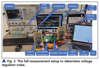
We found that a combination of some of the failed methods would yield good results. For the method proposed in this article (see Figure 2), we used the following two units as the DUT:
- A prototype of Qorvo RFPoL ACT43850 DC-to-DC regulator
- Agilent 33220A AWG signal generator as a known broadband noise source.
- We used the following measurement equipment:
- Agilent E5052B Signal Source Analyzer as a noise density meter (using the “BASEBAND IN” port for direct baseband noise measurement)
- Tektronix MSO64’s Spectrum View as alternative noise density meter
- Picotest High Voltage Noise Bundle
- J2180A-20 preamplifier with the “Shielded” option, as a noise pre-amplifier and to convert the high Z probe to the low Z analyzer. This is a ×10 gain pre-amp, with a high impedance input to 50 Ω output conversion. (Model J2180A is preferable for better low-frequency fidelity, but it was not readily available for testing)
- P2106A-20K-20X 1-port browser probe as a noise probe. This is a near zero capacitance probe to avoid noise due to probe resonance
- SMAJ/SMPMK-500, BNCJ/BNCJ-1000 PDN for high shield attenuation coaxial connections
- Off-the-shelf SMA to BNC conversion adapters.
High Voltage Noise Measurement Outline
The baseline setup of this high voltage noise measurement consists of the following connections:
1. Probe the DUT with the P2106A probe
2. Amplify the P2106A signal and converter and the high Z probe to the 50Ω instrument with the J2180A amplifier
3. Measure the probe and the J2180A amplified signal with a Keysight E5052B SSA using its baseband input port
The internal J2180A DC blocking capacitor is rated for 50 V. Applying 65 V would overstress it and would add noise due to the ferro-resonance. So, we will use the P2106A probe to divide down the entire signal (AC and DC together) of the regulator output by the attenuation of ×1/20. With a combination of ×1/20 P2106A and × 10 J2180A, we have a total × 1/2 gain into the signal source analyzer, keeping the noise gain almost unaffected yet beyond its noise floor, compared to a direct measurement.
Noise Measurement Method Verification
For a detailed, step-by-step validation report, see Reference 1.1 This section includes some of the critical steps.
The first rule of test is to always measure something you know. We start our verification by measuring a known, broadband noise signal generated by the signal generator, with no DC bias. Then, we keep cross-comparing known signal(s) and new signal(s) by doing comparisons of the voltage regulator output noise measurement approaching our goal of the 50 V range and up to 65 V.
It is essential to measure the noise floor for low noise measurements. This ensures high-quality, accurate and repeatable data. We use the signal generator “noise” output mode as a known noise source. The signal generator outputs fixed amplitude vs. frequency white noise up to 10 MHz, and the generator output noise level can be programmed in the unit of mVRMS. When we get the correct noise reading at the signal source analyzer, we can use this measurement as our first correlation point. We use this data to verify the measurement bandwidth and the scaling of the preamplifier and probe.
100 mV RMS Noise Into the Full System
As a full system measurement confirmation, with a known 100 mV RMS signal from the Agilent 33220A, we get the plot in Figure 3.
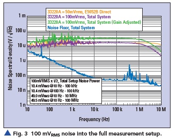
This proposed method has total gain of × 1/2, so the two curves of “33220A = 50 mVrms, E5052B Direct” and “33220A = 100 mVrms, Total system” are expected to overlay, and we confirm that they do.
When we compare this result with the “E5052B Direct,” we see the gain roll off in this measurement, but we can also confirm it is good for our target of up to 100 kHz RMS noise evaluation, and even up to 2 MHz. This bandwidth is mostly controlled by the probe resistance, capacitance of the probe cable, and the input capacitance of the preamplifier.
Measuring DUT DC-DC VR
In the previous sections, we validated the noise measurement setup. Next, we measure a prototype (DUT) DC-DC voltage regulator. As we can directly measure noise outputs up to 35 V directly by the signal source analyzer, we program the DUT VR at 25 V output and compare the two curves (see Figure 4).

By counting the × 1/2 total gain, the two curves of “DUT 25 V, Total System (Gain Adjusted)” and “DUT 25 V, E5052B Direct” are expected to overlay and we confirm they do. We see the curves from this method maintain above the noise floor. We can confirm it is very linear and less additional noise for our target of up to 100 kHz RMS noise evaluation.
We see the slight gain roll-off of this measurement system in the low-frequency region, below 20 Hz. When using the J2180A “Shielded” option, this low-frequency performance is improved with the roll off reduced to 0.1 Hz.
Now, it’s time to measure our target of high output voltage regulator noise. We program the DUT to 50 V and repeat the same steps as above (see Figure 5).
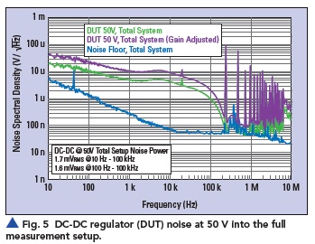
We will reconfirm this curve in the next section.
DUT DC-DC Voltage Regulator at 50 V, Using Another Method
As a correlation purpose, we use one other measurement setup to see if the two 50 V regulator noise measurements are aligned. We use a differential amplifier prototype of Picotest J2103A that is a × 1/6 gain differential amplifier (see Figure 6).

The comparison of two different methods agrees very well with some spurs and gain roll off. The differential probe is noisier than the P2106A and J2180A proposed solution, mostly due to the differential probe’s onboard switching regulators.
Summary and Conclusion
Starting from a known noise signal, and repeating cross-comparison steps, we demonstrated that we can accurately measure 50 output voltage regulator noise with a setup of P2106A + J2180A + E5052B. We see from the broadband noise measurements, shown in Figure 3, that this setup is good for RMS noise measurement up to approximately 2 MHz. The major limitations of the bandwidth are the probe resistance and the cable capacitance.
The proposed P2106A + J2180A solution yielded the lowest noise floor and the most accurate measurement. Other attempts with other non-DC-blocked amplifiers or just voltage divider probes all resulted in higher noise than the proposed solution, non-linear results, or short bandwidth. In the last step, we highlighted in Figure 6 that the P2106A + J2180A + E5052B proposal provides the lowest noise measurement floor.
Reference
1. S. M. Sandler and M. Nogawa, “Measuring High Output Voltage Regulator,” Qorvo Design Hub, Web, https://www.qorvo.com/design-hub.
Published in the SIJ 2022 Print Issue, Technical Feature: Page 18.