
Large ball count, fine pitch BGA parts on a circuit board drive the number of signal layers required to escape the BGA grid into the coarser routing field of that board. Using ultra fine line traces in the BGA escape region will dramatically reduce the layer count for large pin count BGAs. However, using the same ultra fine linewidth traces in the routing field is often at odds with the requirements of achieving a target impedance or a loss spec.
This BGA escape fanout is shown in Figure 1.

Figure 1. BGA escape, top right-hand corner of BGA, showing BGA balls and escape routing.
A common approach to reduce the number of required layers in a board, while meeting a target impedance and loss spec in the routing field is to use narrower traces for routing under the BGA and wider traces in the routing field. This way, the narrower traces can fan out the solder balls to a coarser routing field using fewer signal layers, resulting in a lower-cost board.
With the recent introduction of the Averatek Semi-Additive Process (A-SAP) process, linewidths under 1 mil are possible using the same fabrication processing line as for traditional 4 mil wide lines. An example of these ultra-fine traces is shown in Figure 2
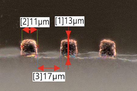
Figure 2 An example of approximately 0.5 mil wide and tall Averatek copper lines showing the capability of ultra fine lines.
This opens up the possibility of using narrower traces in the BGA escape region than in long-path routing regions.
However, using this routing architecture means the narrower traces in the BGA escape field are at a higher impedance than the wider, 50 ohm traces in the routing region. This will result in reflection noise and possible signal degradation on high-speed lines.
If the impedance difference is not too large, or the narrower, higher impedance traces, not too long, this approach may be acceptable. The question is: what is too large an impedance difference and what is too long? What is the design space for the impedance discontinuity of a narrower region, compared to a wider, otherwise uniform transmission line region?
This paper introduces an analysis methodology to explore design space and answer these questions without performing a full system channel analysis of every possible combination of system parameters. This approach is not meant for final design sign-off, but to provide direction and insight into how to engineer mixed-impedance systems to reduce the range of conditions that could be explored in a system-level channel simulation.
While this analysis is done for single-ended impedance, the same process can be applied to differential pairs. The conclusions will be very similar for 50 ohm single-ended as 100 ohm differential traces.
Problem Setup
The design question is really about how long a narrow trace can be, connected to a wide 50 ohm trace, while having acceptable reflection noise? This geometry is shown in Figure 3.
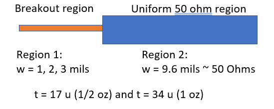
Figure 3. Geometry of two regions. The break out region is the narrower trace, while the uniform region is assumed to be the wider trace.
It is difficult to generalize the answer to the question: how long can a trace be at some higher impedance feeding a 50 ohm trace before the impedance mismatch is a problem?
The transient, reflection noise generated from different impedance regions depends on the rise time of the transmitter, its output impedance, the length of the entire interconnect, the length of each impedance region, the input capacitance of the receiver, and the termination strategy for the circuit. It is difficult to generalize the limitations from just the interconnect given these additional external factors that influence the signal quality at the receiver. (This is also described in the IEEE 802.3 spec in annex 93A, which defines a figure of merit for reflection noise of a channel.)
The new analysis methodology presented here is a simple method offered in the context that sometimes an OK answer NOW! is better than a good answer late.
As a starting place to analyze the limitations imposed by just the interconnect, we use as a metric for the acceptable quality of the interconnect only, the return loss of the channel.
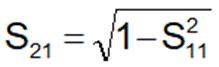
For any lossless interconnect, the total power entering the interconnect must be equal to the power transmitted through and reflected back to the source. As the reflections increase, there will be less power transmitted through. The connection between the transmitted signal, as described by S21 and the reflected signal, S11, for a lossless interconnect is simply,
When the insertion and return loss are expressed in dB, this simple relationship offers considerable insight into how much return loss is acceptable before the insertion loss is decreased by some small amount.
Figure 4 plots the relationship between S21 in dB and S11 in dB, using the above equation. This shows that when the return loss is very small, like -40 dB or even -20 dB, the impact on the insertion loss, S21, is imperceptible, on this scale.
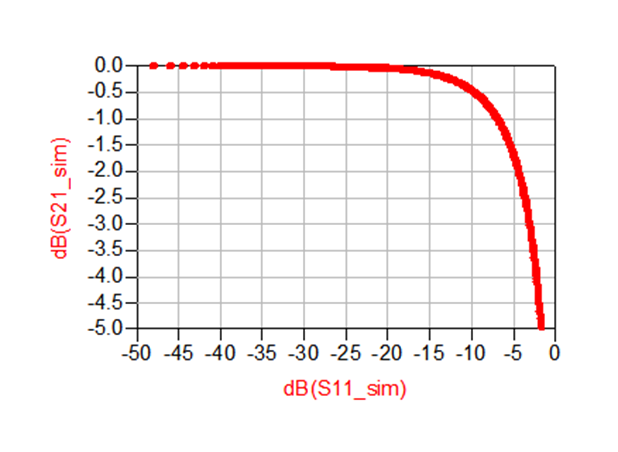 Figure 4. The relationship between insertion and return loss for a lossless interconnect.
In fact, to have an impact on the insertion loss of 0.5 dB requires a return loss as high as -10 dB. This can be used as a metric of how much reflected signal is too much. If the reflections are less than -10 dB, the impact on the insertion loss, the signal at the RX, is virtually unaffected, with only a -0.5 dB drop. This is the origin of the rule of thumb that many connectors are designed for a return loss of less than -13 dB.
Selecting a limiting value of return loss of -10 dB assumes that the largest contributor to the noise budget is just the impedance mismatch between the narrow, BGA break out region trace, and the wider, routing trace. This criterion is a strategic simplification in order to gain some insight in the design space. Near this limit, more detailed analysis should be performed before design signoff.
This is a general methodology and any value of return loss can be selected as a limiting value. The -10 dB value is a starting place.
Exploring Design Space
This problem can be analyzed with a simple, parameterized geometry of a narrower trace, followed by a wide, 50 ohm trace. For this analysis, a microstrip geometry was used, assuming routing on the top layer of the board under the BGA pads.
This circuit was simulated in Keysight’s ADS using the model shown in Figure 5.
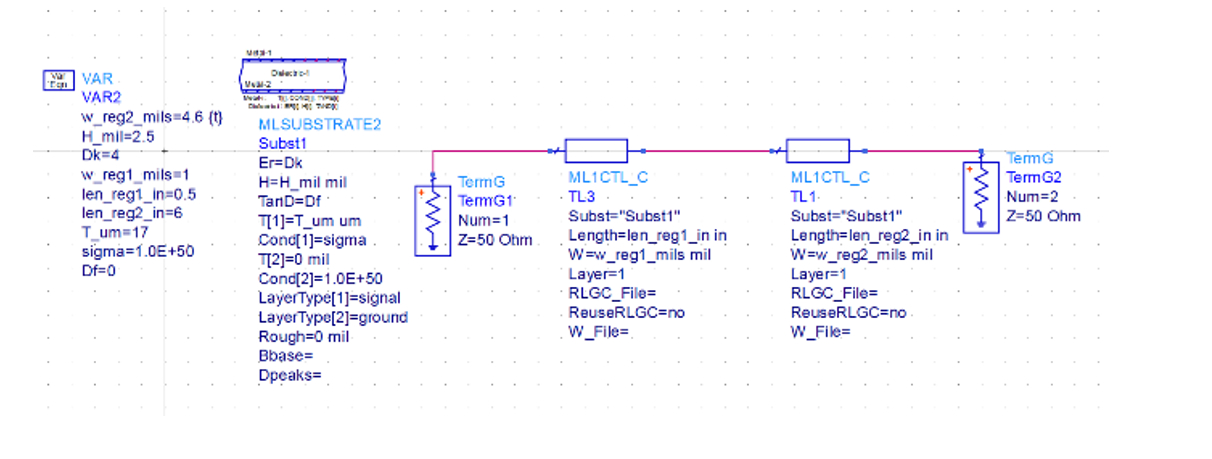 Figure 5. Simulation set up for this two-transmission line structure.
Both transmission lines are routed on the same layer. The second line’s width was adjusted to 4.6 mils for 50 ohms given the dielectric thickness of 2.5 mils and Dk value of 4. Its length was fixed at 6 inches. In this first round, all the interconnects were assumed lossless. A comparison of the worst case with a lossy simulation showed little difference in the return loss from losses.
Given this condition, the simulation could have been done with just the single, narrower transmission line section and the same return loss would have been simulated, since it is surrounded by a 50 ohm environment.
The narrower transmission line’s width and length were varied to explore its impact on the return loss.
As is always good practice, Rule #9 [1] was followed before the simulation was run. We expect that the return loss will be very small at low frequency, as is the case for all sufficiently short discontinuities. As the frequency increases, we will see the reflection increase and then turn into ripples due interference from the multiple reflections from the front and back of the discontinuity region.
If the impedance difference is large enough, there will be some frequency at which the return loss increases above -10 dB. This frequency is a measure of the useful bandwidth of the interconnect.
A longer discontinuity will show a smaller frequency between ripples, and a lower frequency before the return loss increases above -10 dB. A larger impedance difference between the narrow trace and 50 ohms will show more reflections and a lower frequency before the return loss exceeds -10 dB.
The value of the simulation is to provide numerical constraints for the line width when its return loss exceeds -10 dB.
As an example, Figure 6 shows the simulated return loss of two different line lengths of the narrow region, 0.1 inch and 0.5 inches long, up to 20 GHz. Since they have the same value of impedance difference, their peak return losses are the same, but the frequency interval between ripples is different due to their lengths.
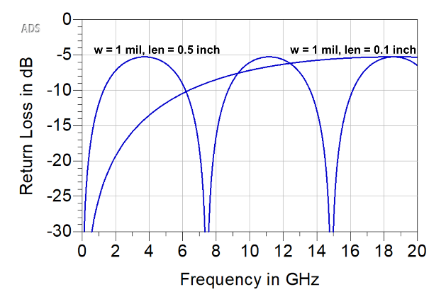
Figure 6 S11, with two lengths for the narrow region,: 0.1 inches and 0.5 inches, simulated up to 20 GHz.
From this curve, we can extract the frequency at which the return loss exceeds -10 dB. We call this the -10 dB bandwidth of the interconnect. For this line width and length, this is the highest useful frequency for this interconnect with a narrow region and a 50 ohm region.
Exploring Design Space Example
Once the dielectric thickness and Dk of the laminate is defined, the width of the 50 ohm region is determined. Then the line width and length of the narrow region can be varied and the -10 dB bandwidth calculated.
The specific design of the board stack up and 50 ohm trace will vary from board to board. In any simulation, we have to start with some specific, defined condition. The value of a parameterized model is that it can be adjusted for any specific conditions.
For this initial simulation, as a starting place, we used the following conditions:
- Dielectric constant = 4.0
- Dielectric thickness = 2.5 mils
- Dissipation factor = 0
- Copper trace thickness = ½ oz = 17 microns
- Line width of 50 ohm region = 4.6 mils
An example of the simulated return loss for the case of a 1 mil wide narrow region, with lengths swept from 0.1 inch to 0.5 inches at 0.1 inch steps, is shown in Figure 7. The -10 dB limit is identified.
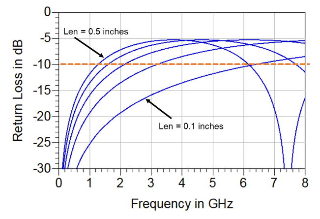 Figure 7. The simulated return loss and -10 dB bandwidth of a 1 mil wide narrow region with five different lengths from 0.1 to 0.5 inches.
Given the fixed stackup, there are only two features of the narrow trace that will have an impact on the -10 dB bandwidth: its length and width. The shorter it is, the higher the -10 dB bandwidth. The wider it is, and closer to 50 ohms, the higher the -10 dB bandwidth.
We summarize the -10 dB bandwidth for three different line widths of 1 mil, 2, mil and 3 mil and five different lengths of 0.1 inch to 0.5 inches in Figure 8.
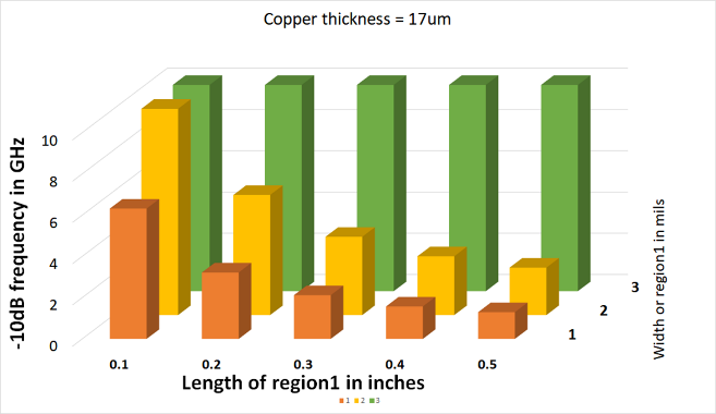
Figure 8. The simulated -10 dB bandwidth for different narrow region conditions in a 50 ohm environment, plotted to a maximum of -10 dB.
This says that given the conditions for the top laminate layer, in a microstrip, the -10 dB bandwidth for a 2 mil wide narrow region that is 0.5 inches long is about 2.3 GHz.
As expected, longer narrow regions have a lower -10 dB bandwidth, and narrow regions with an impedance closer to 50 ohms have higher -10 dB bandwidths.
If the signal bandwidth were 2.3 GHz, corresponding to a rise time of about 0.35/2.3 GHz = 150 psec, a narrow region 0.5 inches long embedded in an otherwise 50 ohm interconnect, might still work. But, if the narrow region were longer than 0.5 inches, there may be the possibility of a reflection noise problem and a detailed simulation should be performed.
When a Narrow Region May Be Transparent
When the narrow region has a different impedance than 50 ohms, there will be reflections in the system. The peak magnitude of the reflections and the worst-case return loss, S11, will only depend on the impedance difference. If the impedance difference is small enough, the return loss will never exceed -10 dB. This would make the narrow interconnect segment effectively transparent, for any length.
The peak return loss as the impedance of the narrow region, Z, is varied compared with 50 ohms can be calculated analytically very simply as 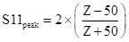
The factor of 2 is there because at peak return loss there is a reflection from the front and back of the narrow region that add together at port 1.
This simple model is compared with the simulated peak return loss for the case of different width narrow regions in Figure 9. The close match adds confidence in both the analysis and the simulation set up.
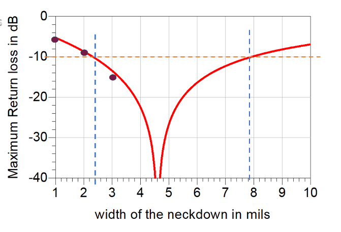
Figure 9 Plot of the maximum return loss as the narrower, neckdown, line width is swept for the case of a 4.6 mil wide 50 ohm trace. The three dots are the analytical model prediction.
This says, if the impedance mismatch of the narrow region is wider than 2.4 mils, while it is an impedance discontinuity, it may still be transparent because the resulting worst-case reflection is smaller than -10 dB.
This analysis was applied to the case of a narrow region with the 50 ohm trace at 4.6 mils wide. If the narrow region were wider than 2.4 mil the narrow region could be any arbitrary length and not bring the return loss above -10 dB. This is shown in Figure 10.
Figure 10 Plot of the return loss for narrow region lengths from 0.1 inch to 3 inches long that are 2.4 mils wide showing that no matter how long it is, the return loss is always less than -10 dB.
The Impact From Losses
The previous analysis was based on using a lossless model for the narrow region and the 50 ohm region. The losses will have an impact on the insertion loss due to attenuation in both regions.
If the 50 ohm region is significantly longer than the narrow region, its losses could dominate the insertion loss. These losses are important and need to be included in the channel analysis.
However, they will not have much impact on the return loss, which is dominated by the reflection noise, not the losses.
To verify this, the worst case was simulated. The 50 ohm region was 4.6 mils wide, and 6 inches long. The narrow region was 1 mil wide and 0.5 inches long. The lossless case was compared with the lossy case using a Df = 0.02 similar to FR4 and the conductor losses turned on. Figure 11 shows these two cases.
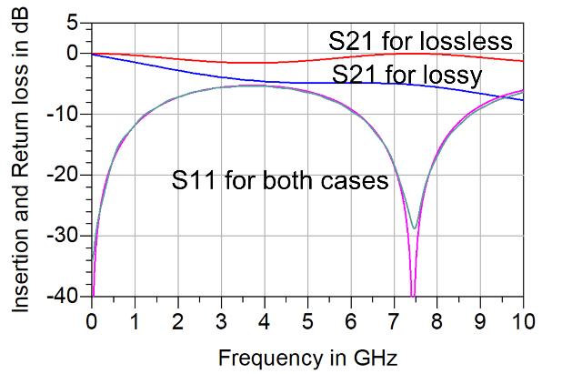
Figure 11. Comparing a lossless and lossy simulation for the worst case. While the insertion loss is affected by the losses, the return loss is unaffected for this worst case.
There is virtually no difference in the return losses for the lossless or lossy cases. This example suggests that the lossless model is a reasonable starting place to explore the impact of reflection noise from the narrow region.
Conclusion
The impact on signal quality from a narrow region in an otherwise uniform 50 ohm trace interconnect will be from reflections. We presented a simple methodology to explore acceptable design space for a narrow region of interconnect.
The impact from its reflections can be kept to an acceptable level if this narrower trace length can be kept short enough. How short is short enough can be estimated with a simple simulation, using the return loss as a simple figure of merit.
In the BGA break out region, it’s possible to use a trace as narrow as half the width of trace in the routing and still achieve acceptable return loss to high bandwidth. This condition could reduce the total layer count in the board. This metric is a useful starting place to consider when narrower traces are needed to reduce the layer count in high layer count boards.
References
[1] Never perform a measurement or simulation without first anticipating the results you expect to see. “Bogatin’s 20 Rules for Engineers” Signal Integrity Journal, January 2020.
Further Reading
Bogatin, Eric. “Return Loss: A Collision Between Two Worlds,” Signal Integrity Journal, April 2020.
Bogatin, Eric. “How Not to be Confused by S-Parameters,” Signal Integrity Journal, April 2020.