
This paper is part 2 in the Ultra-Fine Line Design Guide series. Part 1 is about how small a neckdown is acceptable.
There are three important performance properties of differential pairs that are influenced by the design space of geometry and material properties: differential impedance, channel to channel cross talk, and attenuation. When exploring design space for the optimum design features, all three of these terms are important with different weighing factors, all constrained by the materials available and the fabrication capability of the manufacturer.
This paper focuses on a novel technique of optimizing the geometry and material properties to achieve a target impedance using ultra-fine line microstrip differential pairs as an example. The same methodology can apply to stripline geometry as well. Our subsequent papers will apply this methodology to differential pairs with no return plane, to cross talk analysis, and to attenuation analysis.
A New Range of Features
With the recent introduction of the Averatek Semi-Additive Process (A-SAP™) process, linewidths under 1 mil are possible using the same fabrication processing equipment as for traditional 4 mil wide lines. In this paper we extend the exploration of design space to ultra-fine line features. A special feature of these traces is that their aspect ratio (thickness/width) can exceed 1. But this new geometry realm introduces a set of design tradeoffs.
Methodology to Explore Fine Line Geometries
In this initial study, a differential impedance of 100 ohms is the target, specifically for microstrip transmission lines. The design space for a microstrip consists of the following geometry terms:
- Linewidth, w
- Conductor thickness, t
- Dielectric thickness, h
- Soldermask thickness, h
- Dielectric constant of the laminate, Dk
- Dielectric constant of the soldermask, Dk_sm
The goal in exploring design space is to find a combination of parameter values that optimizes some feature, while maintaining the target impedance.
The challenge for fine line analysis is that the aspect ratio of trace thickness to line width can exceed 1, which means approximations are not suitable for analysis. Only a 2D field solver can accurately calculate the differential impedance. In this study, Keysight’s Path Wave Advanced System Designer, ADS, which has an integrated 2D field solver, was used for the analysis of a virtual prototype. However, this field solver does not display or output the actual differential impedance; it must be teased out from a simulation.
A virtual prototype of a uniform differential pair transmission line was set up with parameterized geometry and material properties. A simulated differential TDR probed the differential pair. From the reflected signal, the differential impedance is calculated for any specific stackup. This circuit is shown in Figure 1.
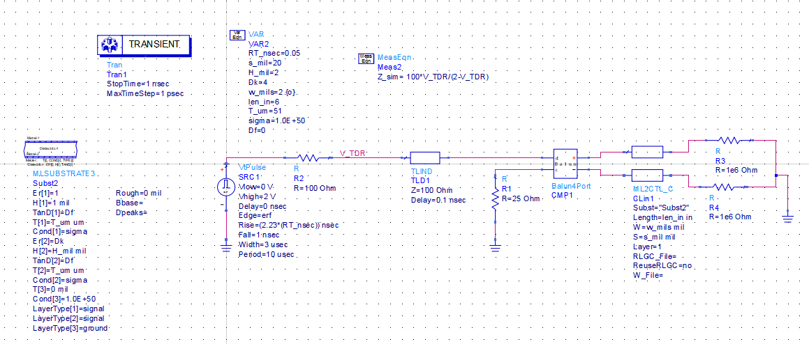
Figure 1. Example of the ADS virtual prototype simulation for a differential pair. The differential pair is defined by its cross-section information and length. The source simulates a TDR, from which the differential impedance is extracted.
This circuit model introduces a number of unique features needed for this analysis:
- All the parameters are set as variables so they can be swept or optimized
- A balun is used to convert an input differential voltage step into the p and n excitation voltages
- The integrated 2D field solver is used to calculate the transmission line response
- The differential impedance is extracted from the simulated reflected signal
- The differential impedance is observed at the middle of the simulated transmission line
- The extracted differential impedance, compared to the target impedance of 100 ohms was used to optimize a specific parameter
- One parameter was selected to sweep, and other parameters were optimized to hit the target differential impedance
The balun in the simulation makes the extraction of the differential impedance very simple. It converts the initial differential step edge signal into the individual p and n signals used to excite the p and n lines of the differential pair. The instantaneous differential impedance is related to the voltage simulated at the V_TDR node from:
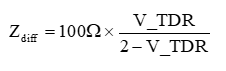
A generic cross section of a microstrip differential pair is shown in Figure 2.
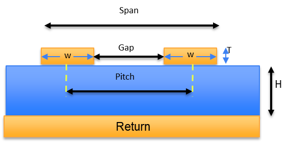
Figure 2. Illustration of the dimension terms used to describe the microstrip differential pair.
Initially, all the parameters were fixed, using the following initial nominal values:
- Linewidth, w = 2 mil
- Gap separation between the inside edges of the two lines s = 2 mils
- Conductor thickness, t = 34 u
- Dielectric thickness, h = 2 mil
- Soldermask thickness, h = 1 mil
- Dielectric constant of the laminate, Dk = 4
- Dielectric constant of the soldermask, Dk_sm = 1 (no solder mask)
This model can be used to illustrate the sensitivity of any parameter on the differential impedance. For example, when the gap separation between the inside edges of the two traces decreases, and all other parameters are kept fixed, we expect the differential impedance to also decrease – but only when the gap separation is small enough to show coupling effects.
This model was used to illustrate this principle. Figure 3 shows the differential impedance as the gap changes and the line width was fixed at 2 mils. When the gap was greater than 10 mils, the differential impedance was independent of the separation, as we would expect. The 10 mil separation corresponds to about 5 x dielectric thickness. This is consistent with the commonly used rule of thumb that the fringe fields from the edge of a microstrip extend to a maximum of 5 x the dielectric thickness. Beyond this distance, there are no substantial fringe fields and no trace-to-trace coupling.
Figure 3. Impact on the differential impedance for fixed 2 mil wide microstrip traces as their gap separation is changed. The dielectric thickness was 2 mils. This is for four different conductor thicknesses.
This simulation also shows the impact from conductor thickness. As the trace thickness increases from ½ oz copper to 2 oz copper, the side wall thickness increases, there is more fringe field from the side walls, and the differential impedance decreases. Since this effect is all fringe field dominated, while we can anticipate the trend, the actual sensitivity on differential impedance from trace thickness can only be calculated using a 2D field solver.
The Johnny Cash Principle
This model can also be used to explore design space by changing one parameter and optimizing another to always achieve a target differential impedance. For example, as the gap separation decreases, to prevent the differential impedance from also decreasing, we can find the optimized line width to achieve the target impedance. In Figure 4 we display the design space for gap separation and line width for a target differential impedance of 100 ohms and 1 oz copper as the gap changes. Everywhere on this curve, the differential impedance of the pair is 100 Ohms. This curve defines acceptable design space.
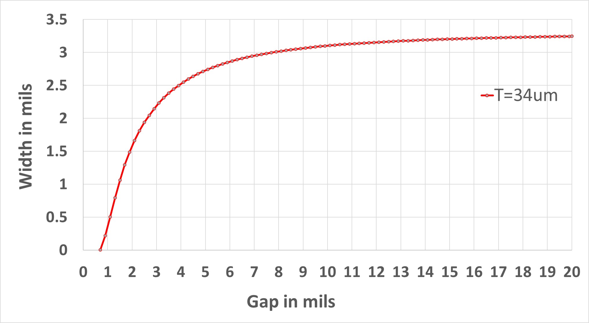
Figure 4. Design space for 100 ohm differential impedance showing the line width required as the gap separation changes for a fixed dielectric thickness of 2 mils and for 1 oz copper traces.