
In this article I show a simple demonstration of how poorly designed interconnects can contribute to near field emissions, which is sometimes an indication of possible EMI failures.
EMI lives in the white space of a schematic
When designing a printed circuit board, we always start with a schematic. All it tells us are the components in use, how they are connected, and what the functionality of the system is. The schematic tells us absolutely nothing about signal integrity, power integrity, or electromagnetic interference (EMI).
Problems with signal integrity, power integrity and EMI all come to life when we turn the schematic into a physical implementation. Once we have connectivity established, the only thing interconnects are going to do is introduce noise and mess with our beautiful design. We follow best design practices to engineer the interconnects so the noise they generate is below an acceptable level.
In this article, I focus on design issues that affect EMI and one way of measuring near field emissions. EMI and electromagnetic compatibility (EMC) refer to a system’s ability to pass a certification test. These tests are all defined in terms of the spectrum of the radiated components, in the far field. Looking at the near field radiated emissions is an important pre-compliance test since this can be done on a benchtop quickly and easily. Looking at near field emissions with a spectrum analyzer can often give a preview of a far field EMC test.
However, sometimes additional insight can be gain looking at the near field emissions using a real time scope. If there is a synchronous signal available to trigger the scope, the impact on emissions from specific signals can sometimes be identified with a real-time oscilloscope. This may point to the root causes of EMI that negatively affect a product’s EMC. Although the oscilloscope does not actually test for EMC, it can be an important tool for pre-compliance EMC testing and debug in both time and frequency domains.
Why EMC Pre-Compliance Testing is Important
There are a number of certification tests for EMC. The one we’ll discuss here, the United States Federal Communications Commission (FCC) Part 15 for Radiated Emissions, tests that a product meets the standard for acceptable far-field radiated emissions for Class A or Class B. The tests are very similar: Class A refers to industrial product environments and Class B refers to consumer environments.
Fundamentally, the product under test is placed in a shielded, anechoic chamber so that there are no sources or reflections from the environment, only the direct radiated emissions from the product. The product is situated one meter above the floor, and an antenna is placed some distance away. This is shown in Figure 1.

Figure 1: Typical set up for an FCC Emissions test.
For Class B, the more stringent test for consumer environments/products, the antenna is 3 meters, or about 10 feet, away. The antenna moves 180 degrees above and below, and 360 degrees around the product looking for the absolute worst case radiated emissions in all orientations as the product is operating normally, scanning with a 120 kilohertz bandwidth detector and sweeping a wide range of frequencies. The test confirms that the peak radiated emissions from the product within that bandwidth across a wide spectrum are below the maximum acceptable electric field levels required by the FCC.
Table 1 shows a few of the maximum acceptable electric field strengths at various frequency ranges for Class B products.
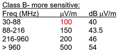
Table 1: FCC maximum allowed radiated emissions for Class B Products operating at various frequencies.
Generally, if a product passes Class B, it will also pass Class A. The Class B criteria for passing at low frequencies, roughly 100 MHz and below, is about 100 microvolts per meter (µV/m). If a product radiates less than 100 µV/m electric field when measured from 3 meters away at frequencies of 100 MHz and below, then it can pass an FCC test. This is a good rule of thumb estimate of what is considered acceptable radiated emissions for a consumer device.
One way to understand what this number means is to imagine a radio station, broadcasting 360 degrees in a spherical pattern (see Figure 2). We stand three meters away from this radio station to measure its electric field strength. If we have a radio source that's broadcasting isotropically, what is the power that must be radiating from that source in order to give 100 uV/m at 3 m distance? Keep in mind that an electric field is an amplitude, not a power. The power is calculated as the square of the electric field.
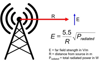
Figure 2: Illustration of a radio station broadcasting into a 120 kHz BW isotropically.
Using the formula in Figure 2, where E is the electric field strength in V/m, R is the distance from the source to where the field is measured in meters, and P is total radiated power in Watts, if we measured 100 µV/m at 3 meters, the total radiated power in Watts is 10 nW. That’s all. So, if a Class B device radiates more than a few nanowatts of power in a 360-degree orientation, it will fail an FCC test required to ship products in the United States.
That’s why it can be so difficult to pass a radiated emissions EMC test, because it doesn't take very much power radiating into that 120 kHz bandwidth of the FCC test to fail, and why there’s so much engineering involved in EMC.
Full FCC-style testing in an anechoic chamber is very expensive. No one wants to submit their product to such a test unless they are fairly confident it will pass, which is why pre-compliance EMC testing is so important for anyone designing an electronic product.
Unintentional Antennas in Electric Circuits
Where do these radiated emissions come from? No one designing a printed circuit board is designing antennas into their product on purpose for unintentional radiation. These sneaky antennas do not appear in the schematic. However, we can unwittingly introduce them into our product with some interconnect features. I often say, “there are two kinds of designers: those who are designing antennas on purpose, and those who aren't doing it on purpose.”
There are two, basic models for antennas—magnetic dipole and electric dipole (see Figure 3). Understanding these antennas will give insight into PCB structures that can radiate.
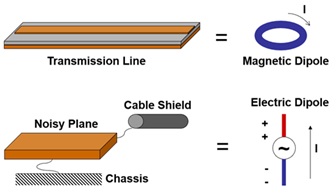
Figure 3. Examples of the two basic types of antennas and PCB structures that behave that way.
Magnetic dipole antennas are comprised of a complete circular loop of current. In typical circuit board applications, all transmission lines and signal-return paths, when done correctly, are magnetic dipole antennas with a signal path and a return path making a complete loop. To keep the impedance controlled, we route the return path directly underneath the signal trace. This keeps the area of the loops small and reduces the efficiency of radiated emissions from magnetic dipole antennas.
Electric dipole antennas have a central voltage source with a couple of wires sticking off each end. When the voltage source creates an AC voltage, we get current sloshing back and forth in those wires. The current must make a complete loop. How does it return between the wires sitting in space? The answer is through the displacement current flowing along the changing fringe electric field lines between the two wires. This is the same path through which current flows in a capacitor.
A perfect example of an unintentional dipole antenna in a circuit board is a noisy ground plane with a coax cable’s shield connected to one end of the plane.
Of course, there is no such thing as uniform voltage on the ground plane. There's always going to be noise on that ground plane, typically called “ground bounce.” The ground bounce voltage can be large or small, so that different parts of the plane are different voltages, which means we have a voltage generator. If one part of the ground plane couples to the chassis, and another part to the shield of an external cable, we've created an electric dipole antenna. Differing voltages on the ground plane will drive common currents onto the cable shield, and those common currents are going to radiate and return through displacement current to the plane or the chassis.
The efficiency of magnetic dipole antennas generally is much, much less than the efficiency of electric dipole antennas. In other words, the same amount of current flowing and returning through displacement current will be much more efficient at radiating from the electric dipole antenna than in a magnetic dipole loop. This is why common currents from electric dipole antennas are going to be the major cause of EMC failures.
Anytime we generate a voltage source that can drive two conductors on either side, we will have radiated emissions if there's an external cable attached to the plane, or even if we have a large enough area on the plane. That's fundamentally what a patch antenna is.
If we have created an electric dipole antenna, we can estimate the far field radiated emissions using this simple approximation:
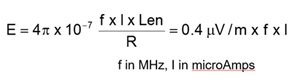
This is the far field electric field strength from the current flowing in a wire, given the frequency, the length of the wire, and our distance from the source. How much common current do we need flowing in that external cable at 100 MHz for the electric field strength to be 100 µV/m at 3 m and fail an FCC test? When you put in the numbers, it is a mere 3 µA. That is not much, which is why we worry about these common currents. They’re the most common source of FCC failures and it doesn’t take much common current to fail an FCC test.
A predominant root cause of common currents is discontinuities in the return path of signals. A return path discontinuity generates a trifecta of problems: it creates reflection noise, crosstalk, and EMI.
If we have ground bounce noise in a ground plane, one region of the plane has a different voltage than another. That's our voltage source. The external wire could be a cable connected to the plane with some common impedance to, literally, the floor. The cable represents a transmission line with the floor as the return. If we have 100 mV of ground bounce noise, assuming a 1 kW impedance typical of 1 m cable over the floor, there would be about 100 µA of common current flowing in the cable shield, way above the 3 µA FCC limit. That's a 4,000 µV/m electric field at 3 m away. This is why it’s so important to lay out circuit boards in a way that reduces ground bounce noise, less to reduce reflections and crosstalk than to reduce EMI.
To reduce the common currents on external shielded cables, the shield should be connected to the chassis. And, to provide a continuous return path for signals, either use a separate return conductor in the shielded cable or also tie the shield to the return plane of the signals.
Near Field vs. Far Field Radiated Emissions
When we are testing a product on our benchtop for EMC, we are in close vicinity to that product in a typically noisy environment. When measuring frequency components in the 100 MHz range and below, 1/10th of a wavelength is larger than 1 foot. When we are closer than 1 foot to the circuit board, all we can measure is near field. It’s important to keep in mind that near field measurements are not the same as the far field (3 m or more) measurements in the FCC test described earlier, and here's why.
When we have some source that's generating radiated emissions, depending on the current distribution and the shape of that source, we will have all sorts of multipole moments radiating: dipoles, quadrupoles, hexapoles, etc. There will be different patterns of electric field radiating based on the pattern of current loops. They all radiate, but the radiation field from the different multipoles drops off with distance at different rates. It's the dipole field that drops off the slowest and survives to the far field. This is illustrated in Figure 4.
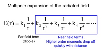
Figure 4. Multipole expansion of near field emissions.
Unfortunately, when we’re close to the product, we’re measuring all the near field strengths, which we may not see in the far field because some of them they drop off so quickly.
That means that we have to be very careful interpreting the results from near field measurements. The near field is going to give us the radiation from all the moments, not just the dipole terms. The downside is that what is measured in the near field is not always a representation of what will be measured in the far field. A lot of near field radiation may not be indicative of a potential FCC failure.
On the other hand, if we fail an FCC test, then we absolutely will see near field emissions, so anything that can be done to reduce the near field emissions will help with passing an FCC far field test, although it is no guarantee.
Testing for Near Field Radiated Emissions in the Time Domain
We can do a simple benchtop measurement of the near field emissions using a real time scope either in the time or the frequency domains. The advantage of the time domain is that if we have a synchronous signal to trigger the scope, we can directly measure the impact from that switching signal or signals switching with it, on the radiated emissions.
In the time domain, we can see the signatures of near field emissions in a way that yields information about the root causes of those emissions. It is a type of pre-compliance EMC testing that can be easily done in any lab, with just about any scope, without the expense of an anechoic chamber.
In this series of experiments to demonstrate a few interconnect structures that cause near field emissions, we used the following equipment:
- A real-time oscilloscope (we used Teledyne LeCroy 12-bit WavePro HD)
- A signal generator
- A current probe (we used Teledyne LeCroy CP30A clamp-on style Hall-effect current probe)
- A magnetic loop “sniffer” probe (or a 10x passive probe looped to create a “sniffer”)
- The DUT
The key to testing in the time domain is to trigger the oscilloscope on some signal that has the potential for influencing radiated emissions, such as a switching signal. If we can trigger on the switching signal, we can find near field emissions that are synchronous with that signal. The time domain is useful in helping us pinpoint exactly when we have emissions, when we have the di/dt in a channel.
The DUT in these examples (see Figure 5) is a 4-layer test board that was designed for one of my classes at University of Colorado, Boulder to demonstrate the effects of ground bounce on radiated emissions.
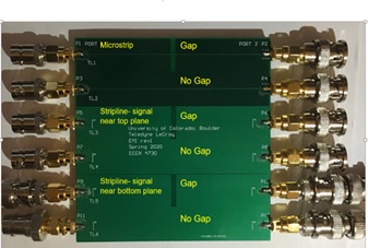
Figure 5. Example of a simple 2-layer test board with return path discontinuities.
There are three sections. Each section contains a pair of traces. The top trace in each section crosses a gap in on or more of the return planes. The bottom trace in each section sees a continuous return plane.
In the microstrip region, one trace runs over a uniform wide plane, the other runs over a gap. This is a classic example of a return path discontinuity. When a signal is sent down the trace that crosses the gap, the return current has to snake back around the gap, forming a loop between the signal and return. The loop inductance in the region of the discontinuity has increased, resulting in a different voltage on the right side of the board than on the left side of the board. As a result, we're going to see radiated emissions from the loop antenna created around the gap by the return current, and from the patch antenna created by the differing voltages on each side of the board.
The signal (generated by a function generator) is a 10 kHz square wave with a 9 ns rise time edge.
The signal passing down the microstrip is shorted at the far end of the line so that the current is going to go back through the return plane and the gap in the return plane.
In order to have a signal to trigger the scope that tells us when the current is passing through the gap, we clamp a current probe onto the (shorting) loop at the far end to measure the current. In our test, about 100 mA of peak-peak current passes through the loop as a square wave (the yellow C1 trace).
The sniffer probe is connected into the scope’s channel 2 using an SMA cable.
We expect to see radiated emissions and near field pick up in the sniffer when the dI/dt passes through the gap. This is synchronous with the return current looping around the gap. It's the di/dt that causes the radiated emissions. With a constant current, we have magnetic field, but it is not changing and not radiating. Using the current edge to trigger the scope, we see the synchronous near field noise in the sniffer probe, in the measurement in Figure 6.

Figure 6. Set up for near field emissions test (right) and results showing resonance (left).
For the best view, we zoom in so that we see only the C1 trigger edge on the screen, with a vertical sensitivity at 20 mA/div and the near field probe, at 50 mV/div. As we move our sniffer probe around the gap in the microstrip, we can see in the pink C2 trace some large magnetic fields that were picked up, inducing a voltage in the sniffer loop. Moving the sniffer probe around the board shows that the emissions are very localized to the discontinuity.
There is also ringing in the C2 measurement. Why do we have that ringing? You should immediately recognize what looks like reflections in a cable.
Let's consider the structure that we have. The low-impedance source loop goes down the trace on the board and induces the di/dt in the vicinity of the gap. The near field emissions induce the voltage in the pickup coil with a low impedance source. That voltage from the coil moves down the 50 ohm cable into the oscilloscope, which is set for 1 MW impedance, so the signal goes from the 50 W impedance of the cable to the 1 MW impedance of the oscilloscope. It's going to reflect, come back, see the low impedance of the short at the other end where the near field probe is, change sign, and bounce back and forth. What we're seeing here is ringing in the cable caused by introducing that low impedance voltage source. We're not really seeing the near field emissions. Rather, we're seeing near field emissions exciting ringing in our cable. That's why terminating the cable in the scope is so important.
When we set the termination to 50 W, the ringing is removed, and what we see are the near field emissions from the structure itself. This is a direct measure of the signature of the near field emissions from this single edge excitation in the trace and the gap in the return path.
Figure 7 shows the near field measurements from the microstrip and two stripline structure with gaps and with no gaps as references.
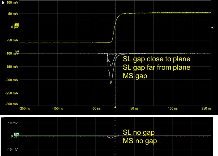
Figure 7. Summary of the near field measurements for the various microstrip and stripline structures for the same dI/dt.
The largest near field emissions is from the microstrip with a gap. With no gap, as seen in the bottom trace, the microstrip emissions are very low, about 1 mV amplitude, compared to 200 mV noise with the gap. When the solid return plane is moved closer to the trace, the impact of the gap in the stripline layer is dramatically reduced. With no gap, the radiated emissions from the stripline are in the noise.
Gaps in the return planes is the common origin of near field emissions from many boards that have a copper fill, for example, on a layer which introduces discontinuities in the return path for signals.
Conclusion
It does not take very much common current to fail an FCC test. The most common cause of radiated emissions failures is common currents from return path discontinuities. These can be measured in the near field with as simple a tool as a real time scope and pick up coil, such as a near field probe. Just watch out for the reflection artifacts in the probe-cable scope system and you can get a clean signature of the emissions from switching currents.
For Further Information
Ott, Henry, Electromagnetic Compatibility, Wiley, 2009
Joffe and Lock, Grounds for Grounding, Wiley, 2010
Paul, C., Electromagnetic Compatibility, Wiley, 2006
Watch this free webinar on Pre-compliance testing using a real-time scope