
The bottom surface profile of the stripline trace and the top surface of the bottom reference plane are the treated matte sides of the foil, shown in the bottom right and bottom left of Figure 5, respectively. They both share the same roughness (Rz3, Rz4 =2.5μm JIS) from the BF-TZA data sheet (see Figure 4).
The next step is to convert the imperial thickness units to metric, then use Equation (1) to determine Dkeff due to roughness for the prepreg and core.


Determine Cannonball-Huray Roughness Parameters
Several popular electronic design automation tools include the Cannonball-Huray model directly as an option, so the respective Rz parameter is all that is needed.
Any of these tools can be used for HLD modeling, but my favorite is Polar SI90009 because of its simplicity and sufficient accuracy for prefabrication modeling and analysis. Many fab shops use this tool for impedance prediction, so it is easy to coordinate with them during the HLD stage of a project. Plus, it has the added benefit of modeling transmission loss and exporting S-parameters in touchstone format for further channel modeling in other tools.
Because Polar Si9000 assumes all the reference planes have the same roughness, it only allows Rz roughness parameters to be inputted for the matte and drum side of the signal trace. The best that one can do, is take the average roughness of Rz1, Rz2 and Rz3, Rz4:


Simulation Correlation
When Dkeff due to roughness values is used instead of published Dk values, the new impedance prediction is 48.24 ohms (see Figure 6).
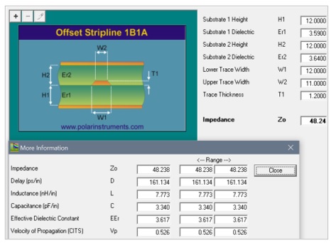
Fig. 6 Polar Si9000 impedance prediction with Dkeff due to roughness.
Dkeff/Df for H1, H2 is then input into the causal dielectric model at 10 GHz (see Figure 7a), while Rzmatte, Rzdrum is inputted into the Cannonball-Huray model (see Figure 7b).
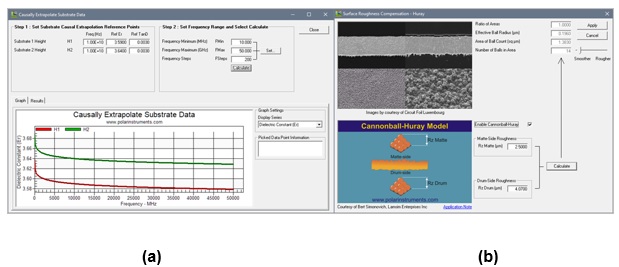
Fig. 7 Causal Dkeff/Df dielectric (a) and Cannonball-Huray roughness model (b) input panels in Polar Si9000.
After a 6-inch transmission line is simulated, the S-parameters are exported in touchstone format. Keysight Pathwave ADS10 is used for further processing and analysis.
Figure 8 compares simulated insertion loss versus de-embedded reflectionless generalized modal (GM) S-parameter measurements, provided by Wildriver Technology.5 Excellent correlation is observed without fitting to measured data!

Fig. 8 HLD insertion loss simulation correlation with measured data for an as-designed stackup from data sheet and stackup parameters.
Figure 9 plots simulated Dkeff versus measurements. At 10 GHz, simulated Dkeff is 0.105 (2.8 percent) lower than the measured value. Without actual cross-section microscopic measurements, it is difficult to conclude if the published Dk is wrong, or if there is process variation with roughness parameters used in the model.
It is interesting to note that measured Dkeff is not a constant value over frequency, as shown in the I-Tera MT-40 Dk/Df tables. Instead, Figure 9 shows that it varies over frequency; so, the Dk/Df data sheet numbers are suspect. Regardless, for the HLD modeling process, the simulation results are within an acceptable tolerance.
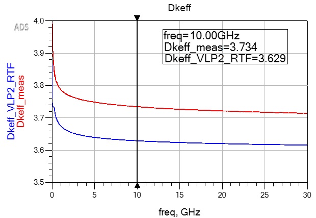
Fig. 9 HLD Dkeff simulation correlation for as designed stackup.
Exploring the Effects of Alternate Foil Roughness
With good correlation to measurements, the HLD modeling process is repeated to explore different foil roughness options. Figure 10 summarizes the thickness of core, prepreg and signal trace for VLP2/VLP2 foil (see Figure 10a) and VLP1/VLP1 foil (see Figure 10b). Note that photos are for illustrative purposes only and are not actual cross-sections from the CMP PCB. Respective Dkeff, and Cannonball-Huray roughness parameters are recalculated using the same steps as VLP2/RTF case above.

Fig. 10 Alternate foil options simulated for what-if loss comparison: VLP2/VLP2 foil parameters for all copper layers (a) VLP1/VLP1 foil parameters for all copper layers (b). (Surface roughness pictures source: Circuit Foil)7
Figure 11 shows the simulation results of all three scenarios. As expected, when the reference plane foil roughness goes from RTF/VLP2 to VLP2/VLP2 there is improvement in insertion loss (see Figure 11a). At 14 GHz the improvement is 0.5 dB and at 28 GHz it is 1 dB.
When VLP1/VLP1 foil is used, there is further improvement (0.8 dB at 14 GHz and 1.7 dB at 28 GHz). For a loss sensitive design, therefore, one might want to consider the VLP1 foil option.
When Dkeff plots are compared, effective Dk approaches actual Dk/Df data sheet values in the tables when smoother copper is used, as expected (see Figure 11b).2 Since Dkeff is derived by phase delay, propagation delay is affected by rougher copper.

Fig. 11 What-if simulation comparison of VLP2/RTF, VLP2/VLP2, VLP1/VLP1 foil options and their effect on insertion loss (a) and Dkeff (b).
Conclusions
Roughness of reference planes make a significant difference in loss and phase delay, especially if one of the reference planes is RTF. If loss is important, then all high-speed reference planes should have the same foil roughness specified.
The heuristic HLD modeling method is a useful and accurate way to determine prefabrication impedance and loss predictions using data sheet parameters.
From the analysis and measurements conducted for this case study, it is found that published Dk from I-Tera MT40 Dk/Df tables is not a flat constant over frequency, and it is confirmed that Rz JIS is the right parameter to use from the Circuit Foil data sheet, instead of Rz ISO.
Acknowledgments
The author would like to thank Al Neves, CTO Wildriver Technology, for providing the custom modeling platform design details and measured data for this case study. He would also like to thank Michael Gay, Director Business Development – Strategic Accounts at Isola Group, for providing foil supplier’s data sheets used on I-Tera MT40 laminates.
References
- B. Simonovich, Heuristic Modeling of Transmission Lines due to Mixed Reference Plane Foil Roughness in Printed Circuit Board Stackups, White Paper, Lamsim Enterprises Inc., June 2021. Web. http://lamsimenterprises.com/Heuristic%20Modeling%20of%20Transmission%20Lines%20due%20to%20Mixed%20Reference%20Plane%20Foil%20Roughness.pdf.
- B. Simonovich, “A Practical Method to Model Effective Permittivity and Phase Delay Due to Conductor Surface Roughness,” DesignCon Proceedings, February 2017.
- B. Simonovich, Practical Method for Modeling Conductor Surface Roughness Using the Cannonball Stack Principle, White Paper Issue 2, Lamsim Enterprises Inc., April 2015. Web. http://lamsimenterprises.com/White_Paper-Practical_Method_for_Modeling_Conductor_Surface_Roughness_Using_The_Cannonball_Stack-Principle-v2.0.pdf.
- L. Simonovich, “Practical Method for Modeling Conductor Roughness Using Cubic Close-Packing of Equal Spheres,” IEEE International Symposium on Electromagnetic Compatibility, July 2016, pp. 917-920.
- Wild River Technology LLC, 8311SW Charlotte Drive Beaverton, OR 97007. Web. https://wildrivertech.com/.
- Isola Group S.a.r.l., 3100 West Ray Road, Suite 301, Chandler, AZ 85226. Web. http://www.isola-group.com/.
- Circuit Foil, 6 Salzbaach, 9559 Wiltz, Grand Duchy of Luxembourg. Web. https://www.circuitfoil.com/portfolio/.
- IPC-TM-650 Test Methods Manual 2.2.17 A, Surface Roughness and Profile of Metallic Foils (Contacting Stylus Technique), IPC, February 2001.
- Polar Instruments Si9000e [computer software] Version 2018. Web. https://www.polarinstruments.com/index.html.
- Keysight Pathwave Advanced Design System (ADS) [computer software], (Version 2021 update2). Web. http://www.keysight.com/en/pc-1297113/advanced-design-system-ads?cc=US&lc=eng.