
Conductor surface roughness has traditionally been applied to copper foil to promote adhesion to the dielectric material. Early PCBs were constructed with only single or double-sided copper core laminates. The one important metric for copper was its purity and the roughness to improve peel strength. There was no such thing as a PCB stackup, and no one worried about impedance or transmission line losses.
Over the years, however, PCBs have evolved into multi-layer constructions with increased attention paid to impedance control and transmission line losses. Thus, a PCB stackup definition is now vital for consistent performance.
For any construction project, a blueprint is needed before building begins. Similarly for PCBs, a stackup drawing and detailed fabrication notes are required. Part of the stackup design process includes signal integrity (SI) modeling for characteristic impedance and transmission loss. If a design is running at 56 Gb/s pulse amplitude modulation level 4 (PAM-4), for example, low loss dielectrics and low roughness copper for the signal traces are likely required.
Sometimes overlooked in the stackup is the roughness of the reference planes. Often thin core laminate power and ground (GND) planes will specify reverse-treated foils (RTF), which are rougher on the side that bonds to the prepreg. Sometimes one of these planes, usually GND, acts as a reference plane to an adjacent signal layer as shown in Figure 1. If that adjacent high-speed signal layer is using smoother copper than one or both reference planes, a higher insertion loss than expected for that layer will occur.

Fig. 1 A stripline cross-section from a stackup showing a thin core laminate (top) with RTF bonded to prepreg adjacent to a high-speed differential pair with smooth foil.
A similar scenario could occur for high density interconnect or HDI technology. This is a popular method to increase component density on modern PCBs. By the nature of the stackup construction, a rougher copper reference plane could sometimes also end up adjacent to a signal layer as well. Thus, if insertion loss is a concern, copper foil roughness of reference planes must be considered.
How is this known before the design stackup and first prototype build? With no empirical data to go by, heuristic, high-level design (HLD) modeling methods are relied on, starting with published parameters found solely in manufacturer’s data sheets. Heuristic HLD modeling is a practical technique that is not guaranteed to be perfect; but, it is still adequate to determine a satisfactory solution sooner, rather than later.
For dielectric parameters, choose a dielectric constant (Dk) and dissipation factor (Df) at or near the Nyquist frequency of the baud rate, then determine the effective Dk (Dkeff) due to roughness.2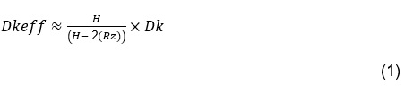 where:
H is the thickness of core/prepreg, Rz is surface roughness of copper, and Dk is the published value in laminate suppliers’ Dk/Df tables. Equation (1) assumes Rz of the foil on each side of the dielectric (core or prepreg) is the same.
For conductor loss, use Rz roughness numbers from copper suppliers’ data sheets and oxide/oxide alternative (OA) Rz roughness numbers from your favorite fab shop, then apply the Cannonball-Huray roughness model.1, 3, 4
Cannonball-Huray Model
The original Huray model is defined as: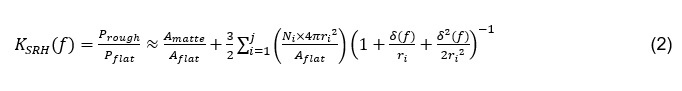
The Cannonball-Huray model allows extraction of the right parameters using Rz roughness for the core and prepreg sides of the foil.1 Because the Cannonball-Huray model assumes the ratio of Amatte/Aflat = 1, and Ni = 14 spheres, the radius of a sphere (r) can be determined by:

and area of a flat tile base (Aflat) is determined by:

Wildriver Isola I-Tera® MT40 Custom Modeling Platform Case Study
To study the effect of reference plane roughness on transmission insertion loss, Wildriver Technology’s custom modeling platform (CMP),5 shown in Figure 2, is used as a case study. This CMP was custom developed for Isola6 to characterize their new I-Tera MT40 very low loss laminate material.
It combines 27 structures based on a consistent development of primitive structures and is useful for performing a host of calibrations including automatic fixture removal, unknown THRU, WinCal XE™ calibration, and VNA gating and time transform analysis.

Fig. 2 Wildriver Isola I-Tera MT40 Custom Modeling Platform. (Source: Wildriver Technology)5
Stackup Validation
The PCB stackup is shown in Figure 3. Often PCB fab shop field application engineers modify existing stackups and unintentionally make errors in transferring new parameters from data sheets into their software tools; also, they may not necessarily know the design intent of the stackup. The first step for any model correlation exercise, therefore, is to sanitize the stackup to ensure it meets the product design intent for SI performance. In fact, that is how the issue of different plane roughness was uncovered.
Since it is good practice to specify the same roughness for both the reference planes and the adjacent signal layers, it was incorrectly assumed that this was the case for any high-speed stackup; however, Layers E1, E2 and E7, E8 specify 1 oz RTF, while layers E3, E4 and E5, E6 specify 1 oz VLP2 foil. Because the Isola I-Tera MT40 CMP is intended to aid in modeling test structures, this is not a fatal flaw. On the contrary, it is a perfect platform to assess the effect of rougher reference planes.

Fig. 3 Isola I-Tera MT40 Custom Modeling Platform stackup. (Source: Wildriver Technology)5
Further review discovered that the core laminates between E3, E4 and E5, E6 specify 1067/2x3313 glass styles, but this combination is not listed for 12 mil thickness. Instead, only 3x3313 core material is offered. Because of that, the Dk shown is also wrong and affects the impedance of the traces. The right Dk for 3 x 3313 is 3.53, not 3.33.
Foil Roughness
As previously mentioned, foil roughness affects the effective Dk, so the right number must be used for model validation. The standard VLP2 foil, used on I-Tera MT40 core laminates is BF-TZA foil. Optional RTF foil, used for layers E1, E2 and E7, E8, is TWLS-B. (Both are available from Circuit Foil.7)
Relevant roughness parameters are shown in Figure 4. For the core side of the foil, the Rz parameters for the treated side are listed; but, there are two Rz parameters, JIS B 601 and ISO 4287. Which one is appropriate for modeling?
IPC-TM-650 Section 1.28 states, “The foil profile of foils shall be evaluated using the parameter Rz (DIN) or RTM, which is defined as the average maximum peak to valley height of five consecutive sampling lengths within the measurement length. This value is approximately equivalent to the values of profile determined from microsectioning techniques.” Section 1.3 states further, “RZ (ISO) is a different parameter from Rz (DIN) and is not applicable to this method.”
Rz JIS represents the 10-point mean value, which is the sum of the average of the five highest peaks and the five lowest valleys over the sample length. Rz DIN is similar; except it is defined as the average maximum peak to valley height of five consecutive sampling lengths within the measurement length. Thus Rz JIS is used for modeling analysis.

Fig. 4 Roughness parameters from Circuit Foil data sheets:7 VLP2 standard foil used on I-Tera MT40 (a), RTF option used for relevant layers in the stackup (b).
Determining Effective Dk Due to Roughness
The first step in HLD impedance modeling is to gather all the dielectric and foil data sheet parameters to determine the effective Dk. Figure 5 shows the core thickness, prepreg and signal traces from the stackup geometry in Figure 3. Note that photos are for illustrative purposes only and are not actual cross-sections from the CMP PCB. Dk for the core and prepreg were obtained from Isola I-Tera MT40 Dk/Df tables.6
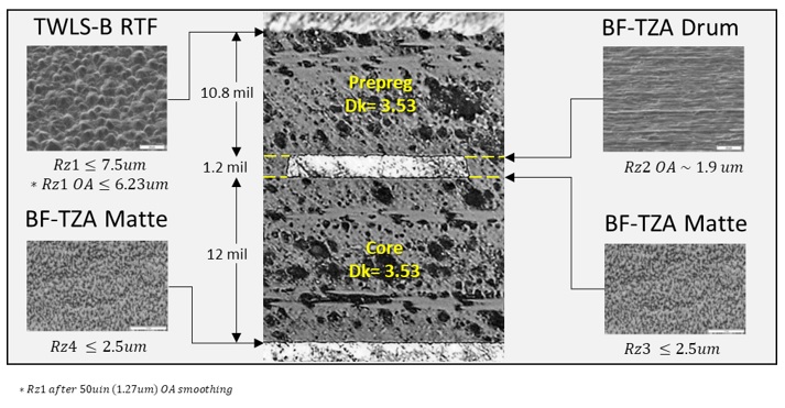
Fig. 5 Data sheet parameters for RTF/VLP2 foil roughness and dielectric properties for the I-Tera MT40 stackup geometry. (Surface roughness pictures source: Circuit Foil)7
The top reference plane is TWLS-B RTF foil with matte side  JIS, obtained from the Circuit Foil data sheet (see Figure 4). The roughness surface profile is shown in the upper left. After OA smoothing,
BF-TZA foil is used for both sides of the core laminate. The top surface of the stripline trace, shown in the upper right picture, is the drum side of the foil before OA treatment. After OA treatment, Rz2 ~ 1.9 μm.1