
Separating RF from Digital in Small IoT Products
Because of skin effect, where high-frequency currents tend to flow along just the surface of a trace or plane, it is possible to use both sides of a return plane to isolate signal or power-return currents. Theoretically, you could run “noisy” signals on adjacent traces above a plane and “quiet” signals on adjacent traces below that same plane, and the two should not couple.
Here is one stack-up idea that uses this concept and has been used successfully by mobile device manufacturers (see Figure 13). If we populate the top side of the board with all the RF/wireless components and the bottom side with the digital, power conversion, and control (while being careful to add return paths to all signals transitioning from top to bottom), field energy from the top should not contaminate the bottom and vice versa.
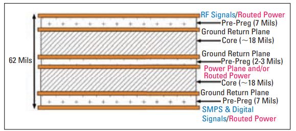
Fig. 13 The concept of partitioning by separating noisy digital circuits on the bottom side from contaminating sensitive RF circuits on the top side.
Note that we keep the main power distribution (usually 3.3 V) in the center of the stack-up. Very complex circuitry or larger layer stack-ups will likely require additional power/return plane layers, which are best located near the top and bottom layers, depending on the number of circuit functions. One recent example I helped with was a mobile video platform with cellular, Wi-Fi, Bluetooth, digital video and audio, and it used a 10-layer stack-up in order to separate functional blocks. Of course, there are many ways to accomplish this objective. Figure 13 is only one example.
Routing Techniques and Other Issues
Gaps in Return Planes: All return planes should be as solid as possible and designed without long gaps or slots (see Figure 14). When a high-frequency trace crosses a gap in the return path, it creates a source of common mode currents, which generally couple all over the board and create the potential for radiated emissions failures and coupling to sensitive receiver modules. See References 2 and 3.

Fig. 14 There are two issues in this example; we have a digital signal crossing two gaps in the ground plane (GRP) and it also crosses a “quiet” analog plane.
The gap also causes field leakage within the dielectric space, which can couple to nearby vias from other signals, causing unwanted coupling. It also causes “edge radiation” directly from the board into antennas. The efficiency of the radiated emissions increases as the harmonic frequency of the common mode currents approaches 1/4 to 1/2 wavelength of either the cables or board dimension. See Reference 11.
Splitting Planes: Many A/D and D/A manufacturers suggest splitting analog and digital planes as a way to isolate digital noise currents from sensitive analog signals (see Figure 15).
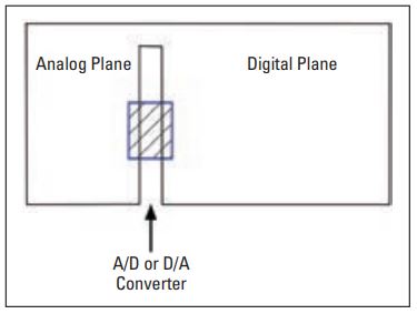
Fig. 15 A split-plane concept is often suggested for A/D or D/A circuits.
This is still an ongoing debate, and my opinion is that there are certain conditions that would warrant this technique, such as low-level audio circuitry in automobile infotainment systems, where you would want the analog return isolated from the digital return. But for most designs, if you use partitioning correctly, it will inherently provide isolation between noisy and sensitive circuit functions, even for A/D and D/A applications. For these latter cases, it is important to keep the analog traces away from the digital traces. Obviously, we do not want to run traces of any kind across the gap.
The real issue when separating planes is that there may be some high-frequency voltage differential between the two. If the planes with their connecting I/O cables approach a significant fraction of a half-wavelength, it can be modeled as a dipole antenna and lead to radiated emissions and various immunity issues (see Figure 16).

Fig. 16 Two separate planes may have an RF voltage potential between them and then radiate like a dipole antenna.
One of the few exceptions (and there are a few others, such as remote sensors) is the need for patient isolation for line-operated medical equipment. Figure 17 shows a typical ground return diagram where the analog probe processing is referenced to analog return, the digital processing circuitry is referenced to digital return, and the power supply is referenced to Earth. The digital and power returns would ideally be connected together at the power connector. The isolation device could be a specialized isolated coupler IC, an optical coupler, or several other similar devices.

Fig. 17 A typical grounding configuration for a patient-connected monitor.
Other Guidelines to Minimize EMI
Clock Oscillators/Crystals/Drivers: These should be located toward the center of the board (or digital partition), as close to the device they are driving, and away from board edges and especially I/O or power connectors.
Clock Traces: all clock traces should be short and direct. Avoid running these along board edges because that can physically couple to the board edge and cause board resonances and consequent board radiation.
I/O and Power Connectors: I/O and power connectors should be located along a single edge of the board and located as close to one another as possible. As connectors are spaced further apart, the chances of increasing EMI-related RF voltage can be measured from one connector body to the other. With cables attached, this can be modeled as an RF source driving a dipole antenna. We want to minimize the RF voltage drop between all connectors by locating them close together. The worst case would be to have connectors located on each side of a board with noisy sources driving common currents to the attached cables.
RF Module Transmission Lines: All antenna transmission lines should be run short and direct to the antennas or antenna port connectors. These may be buried in between two return planes and may dictate eight, or more, layers in order to achieve a 50-Ohm impedance through “keep out” areas in the layers immediately above and below the transmission line(s). Usually, it is best to follow the module manufacturer’s guidance.
Ethernet Connectors: Usually, there should be a void in the ground return (and power) plane directly underneath Ethernet connector magnetics in order to reduce noise capacitive coupling from the board. However, there may be special cases where the connector manufacturer suggests otherwise, especially, if common current-diverting capacitors are included to the return plane under the connector for additional EMI suppression. In that case, the return plane should be extended only up to the capacitors.
Urban Legends
Multiple Decade-Spaced Decoupling Capacitors: Adding a series of (usually) three capacitors, such as, 10, 1, and 0.1 μF capacitors (or similar) on power pins of ICs was thought to help even out the frequency response and lower the overall impedance in the power distribution network. All that actually does is create the potential for parallel resonances due to the various series interconnect inductances (Reference 12). It is best to stick with equal values.
Ground Pours (or Fill): Despite many who recommend this, it is not always a good practice to fill all spaces between signal traces with “ground pours.” It seldom actually helps and there is a chance it could result in higher cross talk due to resonant coupling between traces. (Reference 18).
90-Degree Turns: It has been pretty well proven that for normal digital traces (at least to a few GHz), it is not necessary to chamfer or round off corners. It is all right to make 90-degree bends where needed (References 13, 14, and 15).
20H Rule: There is also the so-called “20H Rule,” where the power plane should be set back from the edge of the return plane by 20 times the dielectric thickness (h). This supposedly helped reduce fringing fields. If nothing else, aligning the planes allows the possibility of adding shorting vias between all the ground planes. (References 16 and 17).
Summary
In practice, designing real PC boards for complex circuits requires some understanding of EM fields. There will always be trade-offs between partitioning of circuits, stack-up decisions, and routing of power and high-frequency signals. However, if the basic design rules are followed:
1. Keep an adjacent return plane for both signal and power distribution layers.
2. Engineer a low impedance return path when transitioning signals through layers.
3. Partition different circuit functions as best you can.
Then you will have a greater chance of keeping noisy signals away from quiet ones, and the risk of radiated emissions, radiated immunity, ESD, and wireless self-interference is greatly reduced.
Most of the projects I’ve been fortunate enough to work on recently have been IoT products, where partitioning and getting the circuit board stack-up and routing designed correctly from the start is so very important for success, not only for reduced EMI, but for proper receiver sensitivity of on-board wireless and IoT receivers.
Remember, high-frequency digital signals travel within the dielectric space, not through the copper. This will dictate the stack-up design. Once you realize this, you can avoid the issue of noisy digital signals sharing the same dielectric space as low-level analog or RF signals and there will be a much greater chance of getting it right the first time.
I’d like to acknowledge the assistance and learnings from physicist, Ralph Morrison (Reference 19), who realized years ago that fields must be considered when designing circuit boards and Rick Hartley, who teaches an excellent two-day seminar on PC board design for low EMI and best signal integrity. I also appreciate the help of Daniel Beeker, senior applications engineer at NXP Semiconductor and Dr. Eric Bogatin, Signal Integrity Journal’s technical editor as well as signal integrity evangelist at Teledyne LeCroy and adjunct professor at the University of Colorado, Boulder, who both helped beat this concept of field theory into my head.
References
1. K. Wyatt, “Characterizing & Debugging EMI Issues for Wireless and IoT Products,” Signal Integrity Journal, July, 2019, https://www.signalintegrityjournal.com/articles/1335-characterizing-debugging-emi-issues-for-wireless-and-iot-products.
2. P. André and K. Wyatt, “EMI Troubleshooting Cookbook for Product Designers,” Scitech Publishing, 2014.
3. K. Wyatt and R. Jost, “Electromagnetic Compatibility EMC Pocket Guide,” Scitech Publishing, 2013.
4. R. Schmitt, “Electromagnetics Explained – A Handbook for Wireless/RF, EMC, and High Speed Electronics,” Newnes, 2002.
5. E. Bogatin, “Signal Integrity – Simplified (3rd edition),” Prentice Hall, 2018.
6. R. Morrison, “Digital Circuit Boards – Mach 1 GHz,” Wiley, 2012.
7. R. Morrison, “Fast Circuit Boards – Energy Management,” Wiley, 2018.
8. R. Hartley, Control of Noise, EMI and Signal Integrity in PC Boards (two-day seminar), Rick Hartley Enterprises, managed by https://www.pcb2day.com.
9. D. Beeker, “Effective PCB Design: Techniques To Improve Performance,” https://www.nxp.com/files-static/training_pdf/WBNR_PCBDESIGN.pdf.
10. H. Ott, “Electromagnetic Compatibility Engineering,” Wiley, 2009.
11. K. Wyatt, “Gaps in Return Planes,” https://www.youtube.com/watch?v=L44lTnQgv-o&t=9s.
12. E. Bogatin, L. Smith, & S. Sandler, “The Myth of Three Capacitor Values,” Signal Integrity Journal, March, 2020, https://www.signalintegrityjournal.com/articles/1589-the-myth-of-three-capacitor-values.
13. H. Johnson, “Who’s Afraid of the Big Bad Bend?”, SigCon, http://www.sigcon.com/Pubs/edn/bigbadbend.htm.
14. Altium, “PCB Routing Angle Myths: 45-Degree Angle versus 90-Degree Angle,” 2018, https://resources.altium.com/pcb-design-blog/pcb-routing-angle-myths-45-degree-angle-versus-90-degree-angle.
15. E. Bogatin, “When to Worry About Trace Corners: Rule of Thumb #24,” EDN, February, 2015, https://www.edn.com/electronics-blogs/all-aboard-/4438573/When-to-worry-about-trace-corners--Rule-of-Thumb--24.
16. H. Chen, et al, “Effects of 20-H Rule and Shielding Vias on Electromagnetic Radiation from Printed Circuit Boards,” archived at SpeedingEdge, https://speedingedge.com/PDF-Files/epep_20hrule.pdf.
17. H. Shim and T. Hubing, “20-H Rule Modeling and Measurements,” Missouri University of Science & Technology (archived at Clemson University), https://cecas.clemson.edu/cvel/pdf/EMCS01-939.pdf.
18. E. Bogatin, “Seven Habits of Successful 2-Layer Board Designers,” Signal Integrity Journal, April, 2019, https://www.signalintegrityjournal.com/blogs/12-fundamentals/post/1207-seven-habits-of-successful-2-layer-board-designers.
19. R. Morrison, https://www.ralphmorrison.com.
Published in the SIJ July 2020 Print Issue, Special Report: Page 24.