
If you can build your product using a solderless breadboard with wires going every which way, and it works, and the interconnects are transparent, then it probably doesn’t matter how you design your circuit board. It will still work. All you need to worry about is design for manufacturing at low cost and maybe design for test. But, if performance matters, if the interconnects are not transparent, or if you want to develop good habits, you will want to incorporate these seven habits in your next two layer board design.
In most 2-layer board designs, performance is limited. Generally, it is hard to route a BGA package such as an FPGA or high-end microprocessor in a 2-layer board. We are not talking high end boards. But, many consumer products, microcontroller and IoT applications are built in 2-layer boards.
In the graduate class I teach at CU, Boulder, on Practical Printed Circuit Board Design, we use the venerable Arduino Uno board as an example of a 2-layer board that works but violates almost every one of the seven important habits. An example of this board is shown in Figure 1.
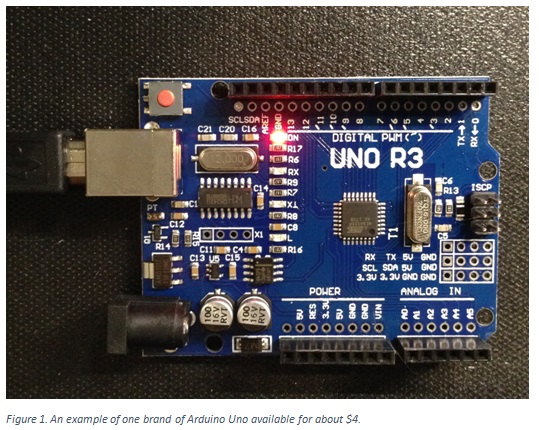
The Arduino Uno is a pretty robust product. You can use almost any design rules and it will work. This unfortunately reinforces bad design habits. In my course we use the Arduino as an example of how NOT to design a board and then re-design it using the following Best Design Practices.
The two problems we are trying to avoid
A schematic identifies the components used in a design and how they are connected. It says nothing about the signal or power integrity performance of the design.
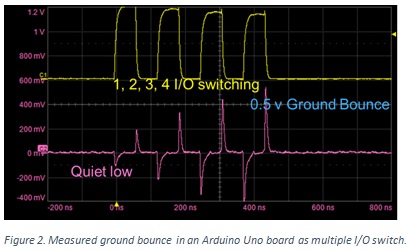
Once the connectivity is established, the interconnects can only screw up the performance of your product. While there are many signal and power integrity problems that can arise, the two most common and with the largest impact, are cross talk due to excessive mutual inductance between signal and return path loops (ground bounce) and switching noise on the power rails due to large transient current swings. Figure 2 is an example of the measured ground bounce in an Arduino Uno board as multiple digital outputs are simultaneously switched on and off.
The goal in the physical design of the board, including the layout, is to follow general design guidelines to reduce these two problems. Without a detailed analysis, which every engineer should do, we can only follow some general design guidelines that will reduce the risk that these problems will bring your product down.
The more analysis you do, the lower the risk and the higher your confidence that your product will work the first time.
There are seven habits we can follow that will not guarantee success but will reduce the risk of failure.
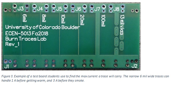
Habit 1: Use 6 mil wide signal trace, 20 mil wide power traces and 13 mil drilled diameter
These are the smallest features every fab house can manufacture at their lowest price. If you keep to these features you can manufacture your board at any fab shop.
You always want to use the narrowest features you can with no extra cost to get the highest routing density. You might think that a 6 mil wide trace is too narrow for a signal line. However, it can carry 1 A of DC current with no discernable temperature rise. Its resistance per length is 80 millliOhms per inch in 1 oz copper. In most applications, a series resistance of even 1 Ohm is still transparent. This is a signal length of 12 inches. Losses don’t play a role until signal bandwidths are > 1 GHz.
The characteristic impedance of a 6 mil wide trace using the standard 62 mils thick 2-layer board will be high, on the order of 150 Ohms. If you have rise times that are short enough or interconnect lengths long enough that require terminations, as long as the traces don’t go off-board, terminations are just as easy to do for 150 Ohm traces as with 50 Ohm traces, and the power dissipation is less.
A 20 mil wide trace in 1 oz copper can handle 3 A of DC current with no noticeable temperature increase. Its series resistance is about 25 mOhms/inch. A power trace 4 inches long has only 0.1 Ohms series resistance, usually not significant. If any power path will carry more than 3 A, increasing to 100 mil wide traces will enable 10 A DC currents.
In the first lab in my class, students test how much current it takes to blow up a trace on a board. They use a simple board, as shown in Figure 3.
Habit 2: Route components, signals and power paths on layer 1 and ground return on layer 2
If the trace has a continuous return path under it, you can make it as long as you want and there will be no impact on performance. The key is to use a continuous return path under the signal line. The easiest way of doing this is to use a solid ground plane on the bottom layer of the board.
This leaves the top layer for all the components, for signal routing and for power routing. It makes debug a little easier to be able to trace the signal routes. And, at a glance, you can tell which traces are signals and which are power by their line width.
Habit 3: Adjust components for less congested routing and space signal traces far apart
Given the component placement, try routing signals as far apart as practical to reduce the line to line crosstalk. The traces have a rather high characteristic impedance. Since they are far away from the return plane, there will be some cross talk between them. The closer the space between adjacent signals, the larger the cross talk. At closest spacing the near end cross talk can be as high as 25%. Spacing the traces farther apart will reduce the near end cross talk.
Habit 4: When you need to route a cross-under on the bottom layer, make it short. When you can’t make it short, add a return strap over it
The goal in best design practices is to provide a low impedance return path for each signal line so that the mutual inductance between adjacent signal-return path pairs is low. When you route a signal line in the ground plane, you have to have an isolation gap around it. The signal traces routed above this gap will see a gap in the return path and generate cross talk to other signals also crossing the gap.
The way to minimize this problem is to keep the gaps short so there is only a short path the return current has to snake around. When it is a long gap, add a return path that jumps over the gap in the top layer. Figure 4 shows examples of gaps from cross-unders with return straps routed in the top layer.

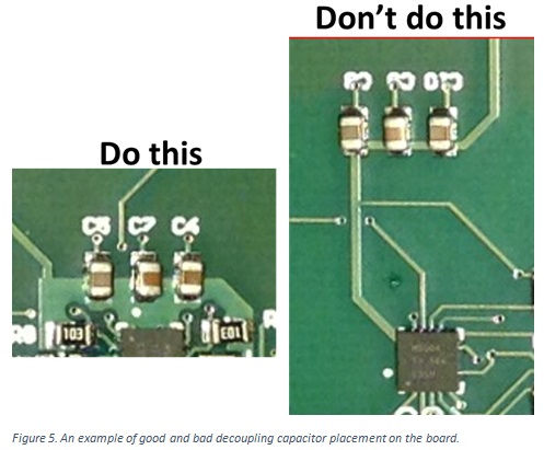
Habit 5: Place decoupling capacitors as close to the power pin of the IC and with as low a loop inductance as practical
Use the largest size capacitor in the smallest body with a voltage rating at least 2x the intended rail application. This is usually a 22 uF MLCC capacitor. The amount of capacitance depends on the current draw of the components you are decoupling. If you are not going to do an analysis, as a rule of thumb, 22 uF will handle a 22 mA of transient current with minimal voltage droop.
The amount of capacitance is not as important as the low loop inductance between the power and ground pins of the IC and the decoupling capacitors. This usually translates into place the capacitors close to the IC pins, and use short, wide traces on both the power and the gnd paths. Sometimes with multiple capacitors, this can be implemented as power puddles. An example is shown in in Figure 5.
Habit 6: On all connectors, try to allocate one return for each digital signal, if possible
A contributing element to ground bounce, or switching noise, is multiple signals sharing the same return pin. In many connectors, there may be only 1 or 2 return pins with multiple signals switching. This is a recipe for ground bounce. This is the case in the Arduino header pins. There is 1 ground pin and 13 digital I/O that can switch. This is one reason there is so much ground bounce.
Habit 7: Don’t follow the two popular guidelines:
- Don’t use three different value capacitors a 10 uF, 1 uF and 0.1 uf for each power pin. There is no problem this solves. And, if not done carefully, it can sometimes add additional problems. If there is room for three capacitors, route them all with low loop inductance and make them all 22 uF.
- Never use copper fill. There is no problem it solves and it can sometimes create additional problems. Instead of using power as a copper fill, route power as traces. This way you can keep track of the power paths to verify connectivity and for debugging. Its from the IC to the decoupling capacitors where low loop inductance is important. Even 10 A of DC current only needs 100 mil wide traces.
If it is a ground fill, use the bottom layer as ground and manage the return paths carefully. Do not rely on a top copper fill for ground. It is too easy to introduce a return path discontinuity and not be aware of it.
Don’t think that adding copper fill that is connected to the ground net will reduce cross talk. If you have continuous return paths that do not overlap, cross talk will be low without any fill. If there is room to add a copper fill between signal traces, the spacing between traces will be large enough to probably have acceptably low cross talk. Unless you treat the fill correctly, it can often increase cross talk, rather than decrease it.
Summary
Following these design guidelines will not guarantee a successful product. They will reduce the risk that a crosstalk or power rail noise problem may cause your product to fail. All of these design habits are free and they will all help reduce risk.
As a final exercise in my class, I have my students re-look at the Arduino board and lay it out using these best design practices guidelines. Figure 6 is an example of what two of my students, Raj Lavingia and Yash Gupte, come up with for a 2-layer version of an Arduino using the Atmega 32U4 microcontroller.
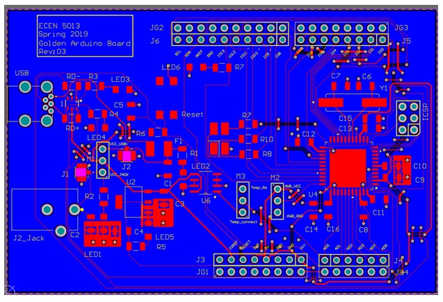
You will note that this design incorporates all of the habits:
- Signals are 6 mil wide, power traces are 20 mils wide, signal vias are 13 mils
- Layer 1, in red, is components, signals and power traces. Layer 2, in blue is a solid ground plane
- Signal traces are spread apart where possible
- In the case of cross-unders routed in the ground plane, gaps are kept short and when they are long, return straps are used.
- Decoupling capacitors are routed close to the power pins with low inductance power and ground loops.
- In the header pins, an additional row of just ground connections is added to the outside of the digital pins. The standard footprint for the Arduino header pins is used, but with the addition of an outer row of pins.
- There is no copper fill on any layer and only one value of decoupling capacitor is used.
In addition to the best design practices for reduced risk for signal and power integrity problems, there are four other important best design practices features added to this board:
- Multiple LED indictors to show power on each rail and some digital functioning.
- Isolation jumpers to isolate power from some circuits for us in debugging
- Multiple test points for signals with adjacent return connections to be used with a 10x probe having a spring tip or coaxial tip
- Liberal use of silk screen information to make it easy in assembly, test and bring up.
Incorporate some of these design habits in your design and reduce the risk and increase your confidence the board will work the first time.