

Introduction
Electromagnetic compatibility (EMC) and electromagnetic interference (EMI) seems to be one of those necessary challenges that must be overcome prior to marketing commercial or consumer Internet of Things (IoT) or wireless products. This transition towards "everything wireless" is in full swing and with it comes problems with EMI. That is, EMI from the product itself interfering with sensitive on-board telephone, GPS/GNSS, and Wi-Fi/Bluetooth receivers. This is called “platform" or self-interference and it’s a big problem for manufacturers.
The proliferation of electronic products, especially wireless and mobile devices, has made compatibility between devices even more important (see Figure 1). Products must not interfere with one another (radiated or conducted emissions) and they must be designed to be immune to external energy sources, such as ESD and RF transmitters.
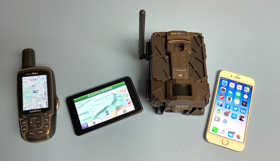 Figure 1. An example of several wireless and cellular devices that can exhibit self-interference, which can affect receiver sensitivity.
In addition, an increasing number of manufacturers are wanting to add or retrofit wireless into existing product designs. These products typically include mobile, household, industrial, scientific, and medical devices. Many of these existing products were not originally designed to accommodate wireless, so result in higher compliance failures than product designed for wireless from the start.
The purpose of this article is to help product designers or EMC engineers learn how to characterize this self-generated EMI so that these issues are addressed early when costs and design changes are minimized. I will follow up with common design issues and mitigations I've used successfully next time.
Wireless Self-Interference
Most digital-based products create a host of on-board radio frequency harmonic “noise” (electromagnetic interference, or EMI), that usually won’t bother the digital circuitry itself. However, that same harmonic energy from digital clocks, high-speed data buses, and on-board DC-DC switch-mode power converters can easily create interference well into the 700 to 950 MHz (and higher) mobile phone bands, causing receiver “desense” (reduced receiver sensitivity).
There are generally two primary areas of focus where on-board noise can couple to the receiver antenna and cause receiver degradation (see Figure 1).
- On-board sources, such as DC-DC converters, address and data buses, and other fast-edged digital signals
- Attached cables that act as “radiating structures” (antennas), such as I/O and power cables

Figure 2. Possible EMI coupling paths include radiated (through air) and conducted (through PC board).
Most coupling modes take place within the PC board itself, due to poor routing and stack-up practices. If there are attached cables, these can radiate directly into wireless antennas.
In order to use the various mobile phone services (Verizon, ATT, Sprint, T-Mobile, and others in the U.S., manufacturers must pass very stringent receiver sensitivity and transmitter power compliance tests according to CTIA (Cellular Telephone Industries Association) standards. This on-board digital noise often delays product introductions for weeks or months.
Cellular and wireless providers require a certain receiver sensitivity in dBm called Total Isotropic Sensitivity, or TIS. For example, this might typically be a sensitivity of at least -108 dBm, and must include the effect of antenna efficiency used in the mobile device. Because mobile device antennas typically operate in close proximity to human hands or head, this tends to reduce the sensitivity further (-99 dBm might be typical, depending on the antenna). More information on this, as well as the test methods, are described in CTIA's "Test Plan for Wireless Device Over-The-Air Performance."1 Cellular radio manufacturer, AT&T, also has some information in their white paper, "Basics of IoT Compliance."2
Broadband and Narrowband
There are two common types of high frequency harmonic plots; broadband and narrowband. Figure 3 shows the difference as we’re looking from 9 kHz to 1.5 GHz. Typically, DC-DC converters or data/address bus data will appear as a very broad signal with several resonant peaks (violet trace), while crystal oscillators or high-speed clocks will appear as a series of narrow spikes (aqua trace). Unless the product is designed for EMC compliance, both these types of signals can radiate or conduct high frequency energy well into the cellular phone or wireless/GPS bands.
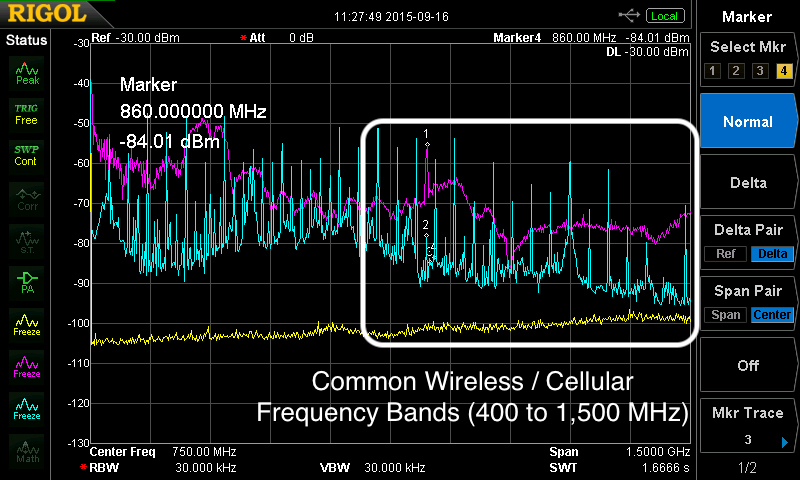 Figure 3. There are two common types of high frequency harmonics: narrowband (in the aqua trace) and broadband (violet trace). The yellow trace is the ambient noise level of the measurement system. It is always a good idea to document a measurement system baseline. The white circle indicates the U.S. cellular LTE and GPS bands.
Characterizing Self-Generated EMI
There are three important steps in characterizing EMI at the board level for an IoT product. We'll describe each step in detail.
- Use of near field probes to help characterize the sources of harmonic energy on the board or system
- An RF current probe to characterize the harmonic cable currents
- A nearby antenna to monitor the actual emissions while troubleshooting. Optionally, you may use a TEM cell in place of the antenna.
Step 1: Near Field Probes
There are three useful measurements for characterizing board-level EMI; (1) a general examination over a wide frequency range and (2) a narrower examination at just the receiver downlink band, and (3) an oscilloscope measurement of the DC-DC converter switched waveform.
The Rohde & Schwarz HZ-15 near field probe kit includes several H-field probes (loops). Since we're wanting to couple to currents in traces and components, that's the type to use. The largest one may be too sensitive and ultimately less resolution. The middle-sized one (model RS H 50-1) is about right to identify and characterize EMI at the board level.
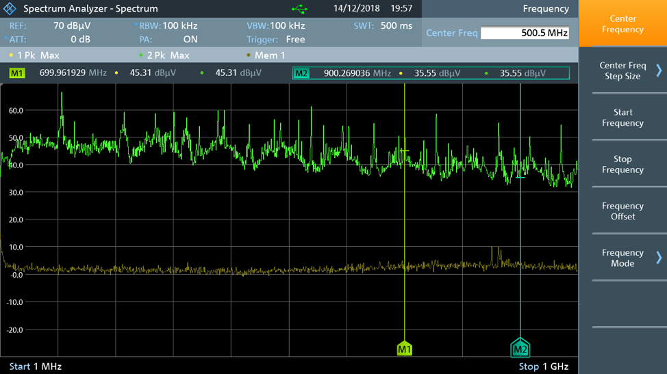 Figure 4. Characterizing the harmonic noise from a DC-DC power converter located on a typical IoT board. The best spot is to couple to the output switching inductor. These are readily identified by their relatively large round package. The probe should be held flat against the inductor for maximum coupling.
Start With a Wide Frequency Span
The wider measurement span helps characterize the general profile of EMI sources, such as DC-DC converters, clock buses, processors, memory, and any other potential high frequency device, such as Ethernet ICs. This measurement is taken from least 1 to 1000 MHz will cover the LTE cellular bands. For PCS mobile phones and/or GPS/GNSS, you’ll need to look as high as 2.2 GHz. For Wi-Fi, you'll need to look as high as 2.5 or 5.4 GHz. Placing the spectrum analyzer in "Max Hold" mode is useful to build up a maximum spectral amplitude.
For example, measuring the processor using the H-field probe reveals a very high level of broadband and narrow band EMI from 1 to 1000 MHz as shown in in Figure 5. Markers 1 and 2 indicate the approximate boundaries of the common U.S. cellular bands from 700 to 900 MHz. The measured EMI (in green) is 30 dB, or more, over the ambient noise floor (in yellow).
 Figure 5. In this example, we’re using the Rohde & Schwarz FPC1500 spectrum analyzer and looking from 1 to 1000 MHz to generally characterize the spectral emissions profile of the processor (green trace). The yellow trace indicates the noise floor of the measurement. The U.S. cellular band for is generally indicated with markers M1 and M2 at 700 and 900 MHz. This processor EMI will potentially cause interference if it coupled to the cellular receiver.
Narrow the Span to the Downlink Band
Once the various noise sources on the board are identified, the second useful measurement is to narrow the span and look at just the receiver (downlink) band using the same near field probe. For example, the downlink band for Verizon in the U.S. would be "Band 13" of the FCC allocation from 746 to 756 MHz (see Figure 6).
You may need an external broadband preamplifier of at least 20 to 30 dB gain in order to clearly observe the noise, if any. If your analyzer has an internal preamplifier (usually 20 dB gain) that should suffice. Rohde & Schwarz also sells a separate high-gain broadband preamplifier with low noise figure. You may need to make these measurements inside a shielded room in order to exclude other mobile phone transmissions from disrupting your measurements.
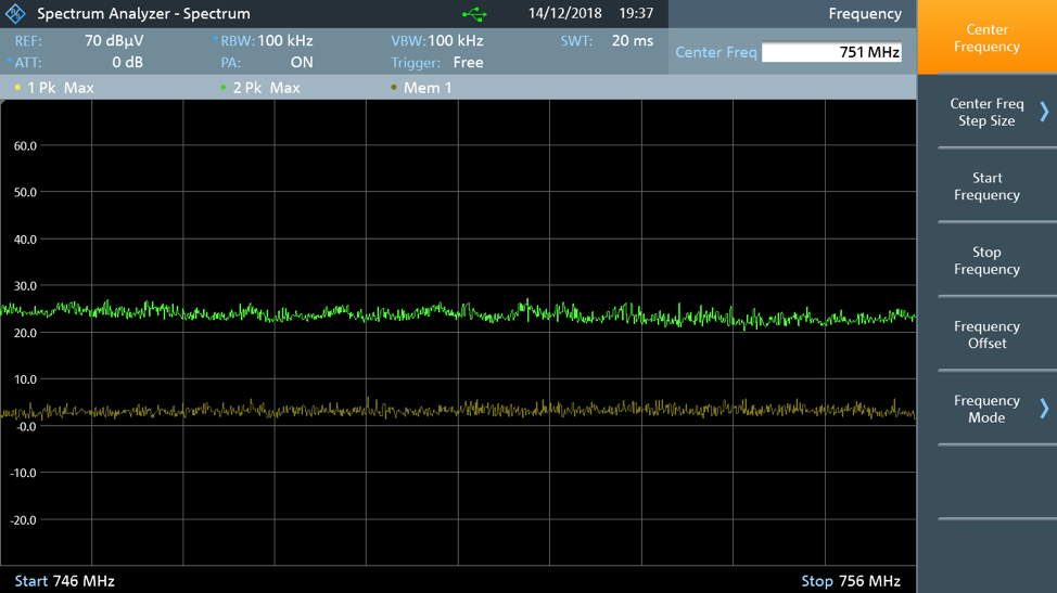 Figure 6. Measurement of the DC-DC converter (green trace) within the receiver downlink band for Verizon Band 13 (746 to 756 MHz). Note the broadband noise in the green trace is about 20 dB above the ambient noise floor. The yellow trace is the ambient system noise floor measurement.
Characterize DC-DC Converter Ringing and Rise Times
The third useful measurement using the H-field probe is to characterize the switching waveforms of the various DC-DC converters in the time domain. This is important for identifying ringing on the switched waveform, because this ring frequency can translate to broad peaking in the emission characteristics. H-field probes are quick and safe because they don't require direct connection to the circuitry - just couple it to the output switching inductor.
In order to show this to be a valid characterization measurement, and referring to Figure 7, let's examine the math. There will be some unknown mutual coupling factor (M in the equation below) between the inductor and H-field probe. Because we don't know the mutual coupling factor the amplitude won't compare with actually measuring with an oscilloscope probe. However, for EMI purposes we're mainly interested in the rise time, general switched wave shape, and ringing frequency, if any. See Figures 8 and 9 for an example comparison between the switched waveform characteristics from a RT-ZS20 oscilloscope probe and the RS H 50-1 H-field probe showing that the measured EMI-important results are generally identical.
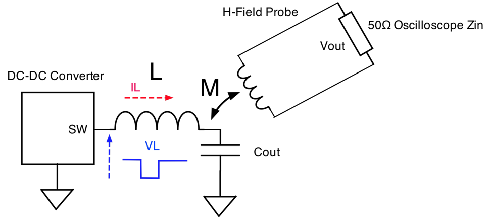 Figure 7. Modelling the switched waveform between the output inductor of a DC-DC converter and H-field probe.
A DC-DC converter usually has a near square wave signal (VL) from the converter switch node (SW) and output inductor (L) input to ground return and this is what we'd measure with an oscilloscope probe. The current through the inductor is related to that voltage as:
Assuming the H-field probe is held close to the inductor, we get some mutual coupling, M (unknown) and the output of the probe is:
Combining these two equations, we get:
Therefore, factoring out the constant, M/L, we see Vout∝VL.
Because Vout is proportional to VL the most important characteristics for EMI are now easily and quickly measured without the risk of shorting connections with oscilloscope probe tips during circuit operation. By using the H-field probe held close to each DC-DC converter inductor, we can measure the rise time (indicates the upper range of harmonic frequencies), pulse width and period (also factors into harmonic frequencies), and ringing frequency (which can cause broad resonant peaking in the broad band spectrum. See Figures 8 and 9 for a comparison between measuring with scope and H-field probes.
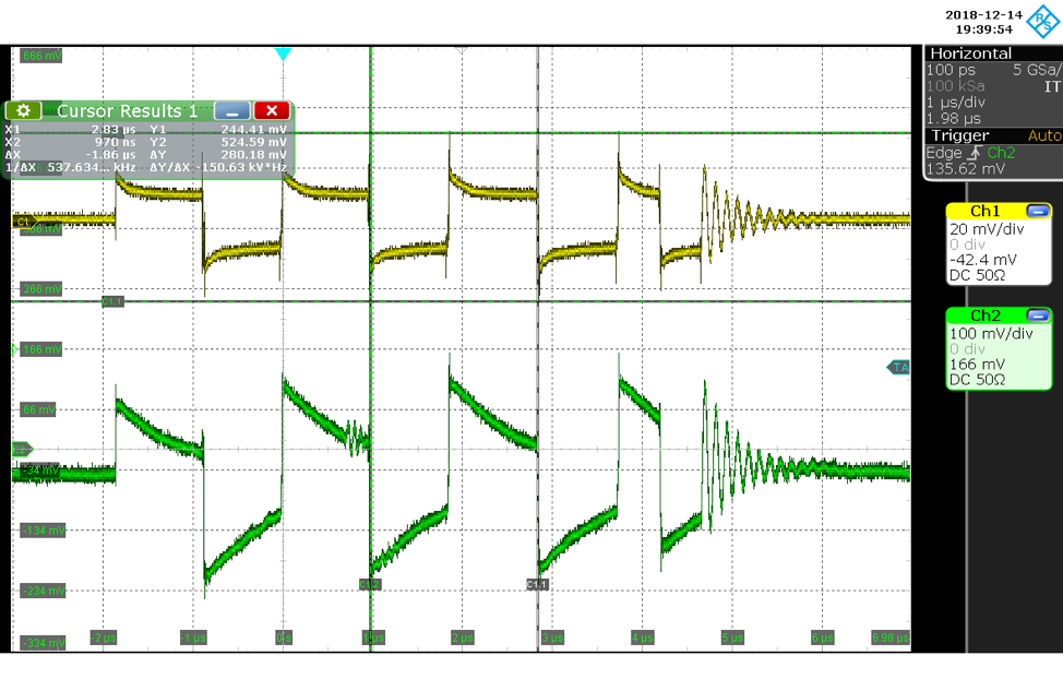 Figure 8. Probing the DC-DC converter output inductor L1, showing the coupled H-field probe and direct-connected single-ended probe show similar waveforms. By using the H-field probe, measurements like rise time, period, and ringing may be observed quickly and without risk of shorting circuits with oscilloscope probe tips.
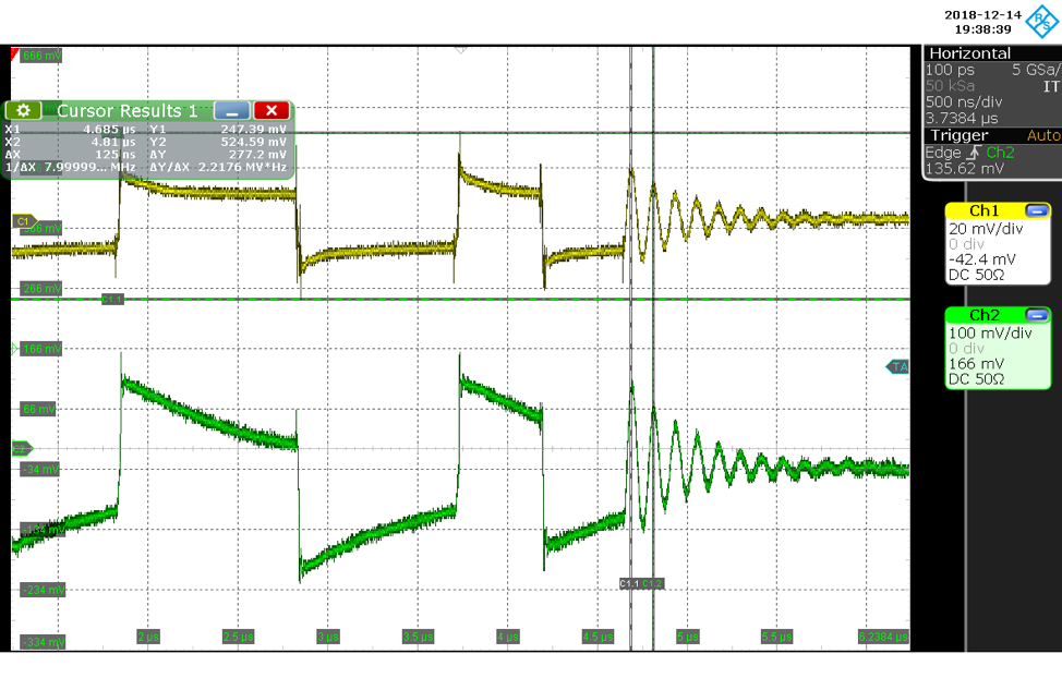 Figure 9. Measurement of the ringing on the DC-DC converter. This could translate to broad peaking in the EMI at 8 MHz (plus higher-order harmonics).
Step 2: Current Probes
Figure 10 shows how a current probe is used to measure the common mode harmonic currents flowing along a power cable. How these currents are formed and why they tend to couple onto cables is explained in Reference 4. Let's just say that small RF common mode currents generated on the PC board (usually in the µA range) can easily couple to attached I/O and power cables, which can then re-radiate into the radio module antennas as we saw modelled in Figure 2 previously.
An oscilloscope with an FFT feature, such as the Rohde & Schwarz RTE- or RTO-series oscilloscopes or a spectrum analyzer is the most useful tool for these measurements, as entire frequency spectrums may be observed. The current probe can measure RF common mode currents in the in either power cords or I/O cables. Either can radiate directly to IoT antennas.
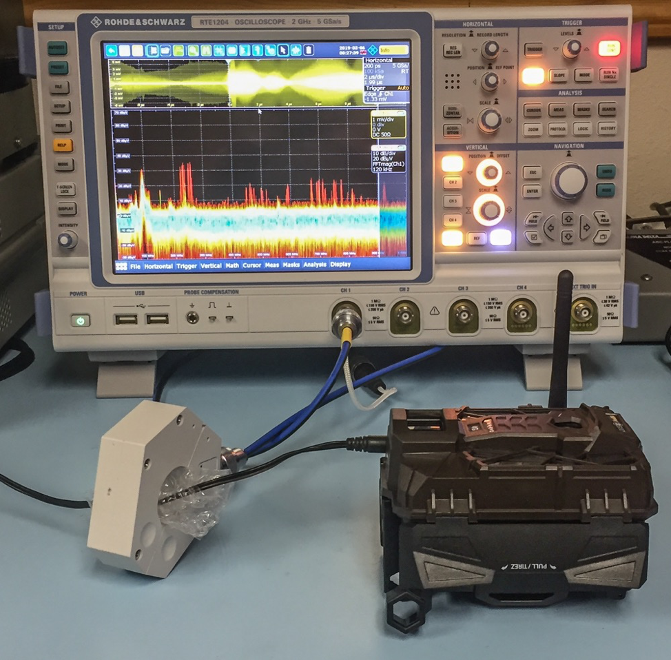 Figure 10. A high frequency R&S EZ-17 current probe is being used to measure the power cable harmonic currents coupled from the PC board of Device 1 (wildlife camera). (Image courtesy Wyatt Technical Services.)
All commercial current probes, such as the Rohde & Schwarz EZ-17, have a calibration chart included that shows the transfer impedance (usually dBΩ) versus frequency (see Figure 11). The nearly flat horizontal linear region is the most useful part of the plot, as you can use a constant transfer impedance to calculate the common mode current in the measured wire or cable.
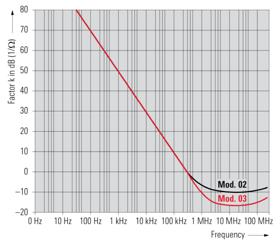 Figure 11. The transfer impedance versus frequency for the Rohde & Schwarz model EZ-17 current probe.
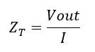
Where Vout is the measured voltage at the 50 Ω port and I is the common mode current in the wire or cable.
We can express this equation in dB:
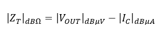
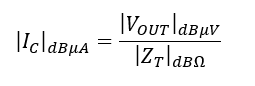
Solving for I (common mode current through the wire or cable):
One very interesting outcome, is that knowing the common mode current traveling in a wire (assuming the length is electrically short compared to a wavelength), we can calculate the expected E-field from this wire or cable, based on the following equation:3,4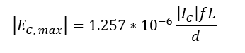 Where Ec,max is the calculated E-field (V/m), Ic is the measured common mode current (A), f is the harmonic frequency (Hz), L is the length of the wire or cable (m), and d is the measured distance from the wire or cable in m. Typically, d would be 3 m or 10 m is used for radiated emissions compliance test in order to compare with test limits in commercial EMC standards.
The ability to calculate the approximate pass or fail, given the harmonic current measurement of a wire or cable is a powerful tool when dealing with radiated emissions from a product.
While this ability is not as important when dealing with near-field emissions directly into sensitive IoT receivers, it is still nice to know, relatively-speaking, whether a given power or I/O cable might be contributing to the overall noise coupling or radiated emission issue.
Step 3: Close-Spaced Antenna
To measure the direct emissions from a PC board with or without cables attached, you may use a close-spaced antenna to pick up the emissions. The antenna does not need to be calibrated or even resonant over the entire frequency range, just positioned at a close enough distance where harmonic emissions may be observed. You may the antenna will need to be positioned closer than 1m to observe the emissions (see Figure 12).
The most important harmonic frequencies to monitor would include the cellular LTE bands (approx. 700 to 900 MHz, the commercial GPS L2 frequency of 1575.42 MHz, the higher cellular bands around 1.8 to 1.9 GHz, and the Wi-Fi ISM band of 2.4 to 2.5 GHz. On-board harmonic content seldom goes higher than that.
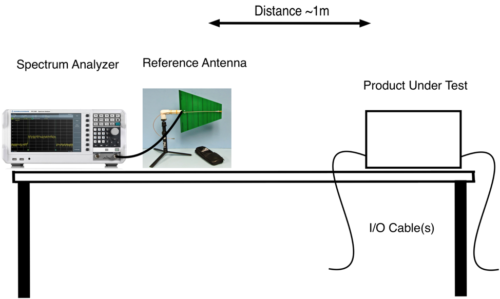 Figure 12. A typical test setup to characterize the actual radiated emissions from an IoT product (or any product for that matter). The test distance or a calibrated EMI antenna is not critical, as the important thing is to be able to observe the harmonic emissions.
Step 3: TEM Cells (Option)
An alternative to setting up an antenna would be to use a TEM cell to characterize the emissions from a bare IoT board or product, assuming it will fit within the septum area.
In order to measure the direct emissions from a PC board with or without cables attached, it may be placed into a small TEM cell (see Figure 13), such as the ones manufactured by Tekbox Digital Solutions.7 A TEM cell is simply an expanded 50 Ω transmission line. Placing an operating test board (protected with an insulator) within the septum area can capture the general emission profile.
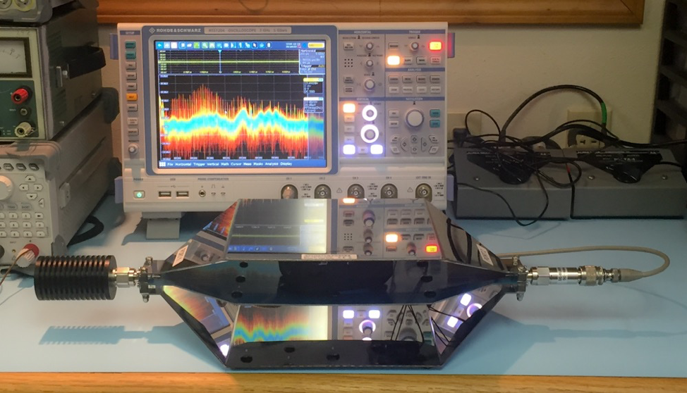
Figure 13. A TEM cell, such as this model TBTC2 by Tekbox Digital Solutions, may be used to evaluate radiated emissions from small IoT boards.
In use, connect a 50Ω termination to one port of the TEM cell and a DC block to the other end for protection of the oscilloscope or spectrum analyzer in case DC voltage ends up on the septum plate. Then connect a coaxial cable from the DC block to the oscilloscope or analyzer input and adjust for the desired frequency limits (see Figure 14).
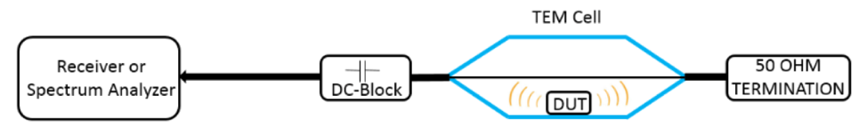 Figure 14. General test setup for measuring radiated emissions from a small product. (Image courtesy Tekbox Digital Solutions.)
Because of the open TEM cell design, this test may also have to be performed in a shielded room in order to exclude strong ambient RF signals from broadcast stations, television, or cellular transmitters.
Any attached cables may also pick up ambient signals from radio, television, two-way radios, or cellular phone. If that's the case, try attaching several equally-spaced ferrite chokes along each cable. In any case, it is best to record an ambient plot over the frequency range being measured to help identify and distinguish between ambient and board-generated signals. If the IoT product can be powered from batteries, that's even better, as the cables may be eliminated.
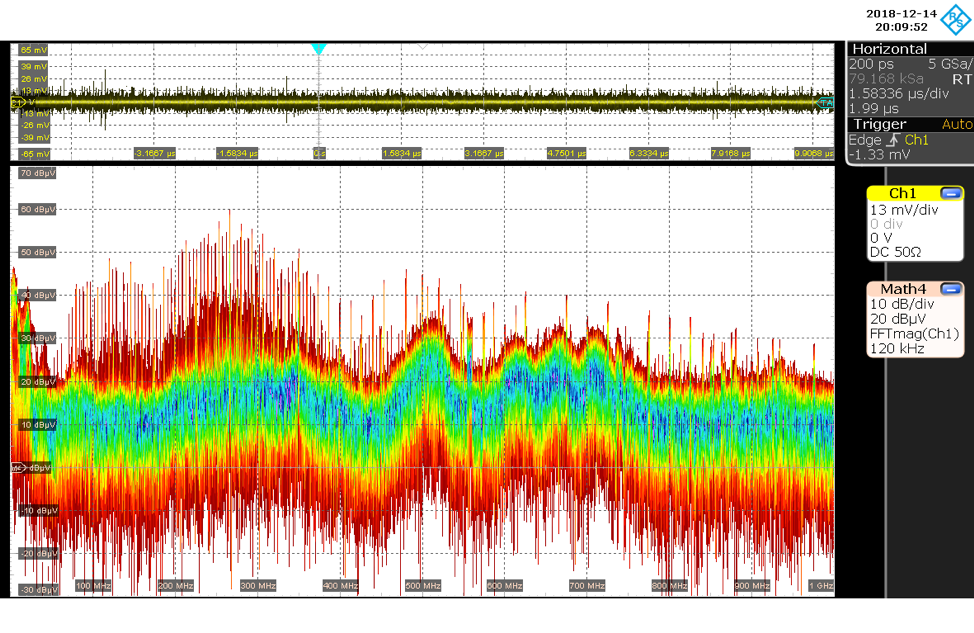
Figure 15. The emissions as measured in the TEM cell. Note the combination of both narrow band and broadband emissions extending out to 1 GHz.
Figure 15 demonstrates the radiated EMI. While not directly comparable to formal radiated emission limits, this will still provide valuable information on where the highest EMI frequencies lie and whether any major emissions could be coupling directly to wireless or cellular antennas.
Summary
This article has described three steps I use for characterizing wireless self-interference, using near field probes, RF current probes and a close by antenna to help determine radiated couplings. Any emissions that encroach into the receiver downlink band will likely cause some level of receiver desense. Once the various energy sources are identified by using a combination of near field probe, RF current probe and nearby antenna, then troubleshooting may commence.
In the next installment, I will discuss what I have found to be the most common design issues and describe several mitigation techniques that have worked for some very challenging wireless products.
REFERENCES
- CTIA, "Test Plan for Wireless Device Over-The-Air Performance."
- AT&T, "Basics of IoT Compliance."
- Ott, Henry W., Electromagnetic Compatibility Engineering, Wiley, 2009.
- André, Patrick G. et al., EMI Troubleshooting Cookbook for Product Designers, SciTech, 2014.
- Würth Electronik, Trilogy of Magnetics, 5th edition, 2018.
- Rohde & Schwarz, EZ-17 current probe.
- Tekbox Digital Solutions, "Open TEM Cells for EMC Pre-Compliance Testing."
- Kevin, Slattery et al., Platform Interference in Wireless Systems - Models, Measurement, and Mitigation, Newness Press, 2008.