
An increasing number of manufacturers are adding or retrofitting wireless technology into new or existing products. These products typically include mobile, household, industrial, scientific, and medical (ISM) devices. This transition towards “everything wireless” is in full swing, and with it comes problems with electromagnetic interference (EMI) from the product itself interfering with sensitive on-board cellular, GPS/GNSS, and Wi-Fi/Bluetooth receivers. This is called “platform” or self-interference, and it has become a big problem for manufacturers.
Wireless Self-Interference
Most of today’s digital-based products create a large amount of on-board RF harmonic “noise,” or EMI. While this digital switching will not usually bother the digital circuitry itself, that same harmonic energy from digital clocks, high-speed data buses, and especially on-board DC-DC switch-mode power supplies can easily create interference well into the 700 to 950 MHz (and higher) cellular phone bands, causing receiver “desense” (reduced receiver sensitivity). In order to use the various mobile phone services (Verizon, ATT, Sprint, T-Mobile, etc.), manufacturers must pass very stringent receiver sensitivity and transmitter power compliance tests according to CTIA (Cellular Telephone Industries Association) standards. This on-board digital EMI and resulting receiver desense often delays product introductions for weeks or months.
Cellular and wireless providers require a certain receiver sensitivity in dBm called total iso- tropic sensitivity (TIS). For example, this might typically be a sensitivity of at least −108 dBm, and must include the effect of antenna efficiency used in the mobile device. Because mobile device antennas typically operate in close proximity to human hands or head, this tends to reduce the sensitivity further (−99 dBm might be typical, depending on the antenna). More information on this, as well as the test methods, are described in CTIA’s “Test Plan for Mobile Station Over the Air Performance: Method of Measurement for Radiated RF Power and Receiver Performance.”1 Cellular radio manufacturer, Broadcom, also has some information in their white paper, “Compliance with TIS and TRP Requirements.”2
Characterizing Platform (or Self-Generated) EMI
Let’s now look at how to characterize this self- generated EMI and then describe some possible mitigations. There are generally two primary areas of focus where on-board energy sources can couple to the receiver antenna or wireless module and cause loss of receiver sensitivity (see Figure 1):

- On-board energy sources, such as DC-DC converters, ad- dress and data buses, and other fast-edged digital signals that can conduct or couple this EMI directly to wireless modules or their antennas.
- Attached I/O or power cables that act as “radiating structures” (antennas) that couple this self-generated RF energy directly into on-board or attached wireless antennas.
There are three measurement techniques you can use to characterize platform interference:
- Near field magnetic or electric field probes for locating dominant energy (EMI) sources.
- High-frequency current probes can be used to measure small RF currents on I/O and power cables.
- A nearby antenna or TEM cell for measuring the actual near field emissions directly from the PC board or attached cables.
Given these characterization techniques, it is often possible to determine the sources of electromagnetic energy that could be coupling to on-board wireless receivers. Once the energy sources are identified and characterized, then the challenge is to determine how that energy is being coupled into the receiver and applying mitigating techniques for reducing this coupling.
Very often, the EM fields are coupled directly within the board, due to poor stack-up, poor functional circuit compartmentalization (RF, digital, power conversion), or poor signal/ power routing. It is also very possible that stray electromagnetic fields are simply coupling directly into the antenna. It could also be a combination of both.
Types of Interference
The two common types of high-frequency harmonic signals that can disrupt sensitive receivers are narrow band and broadband. Figure 2 shows the difference as we are looking from 1 to 1500 MHz. Typically, DC-DC converters or data/ address bus data will appear as a very broad signal with several resonant peaks (violet trace), while crystal oscillators or high-speed clocks will appear as a series of narrow spikes (aqua trace). Unless the product is designed for EMI compliance, both these types of signals can radiate or conduct high frequency energy well into the mobile phone or other wire- less bands.


Both sources of EMI will potentially cause interference to the U.S. 700 to 900 MHz cellular and GPS bands, indicated by the area enclosed by the white circle. The aqua trace has peaks that are more than 40 dB over the ambient noise level within the cellular band.
Types of Measurements
Three methods have been developed to diagnose self- interference for IoT-enabled devices: use of near field probes to help characterize the sources of harmonic energy on the board or system; a current probe to characterize the harmonic cable currents; or a nearby antenna to monitor the actual emissions while troubleshooting. Optionally, you may use a TEM cell in place of the antenna.
Step 1: Near Field Probes
There are three useful measurements for characterizing board-level EMI, notably: a general examination over a wide frequency range; a narrower examination at just the receiver downlink band; and an oscilloscope measurement of the DC- DC converter switched waveform.
For near field measurements, an H-field loop with about a 1 cm diameter is about the right size to identify and characterize EMI at the board level (see Figure 3).
Start With A Wide Frequency Span
A wider measurement span helps characterize the general profile of EMI sources, such as DC-DC converters, clock buses, processors, memory, and any other potential high- frequency device, such as Ethernet clocks. This measurement is taken from least 1 to 1000 MHz and will cover the U.S. cellular LTE bands. For other mobile phone and/or GPS/ GNSS, you will need to look as high as 2 GHz. For Wi-Fi, you will need to look as high as 2.5 or 5.4 GHz, but these on-board emissions seldom extend above 2 GHz. Placing the spectrum analyzer in “Max Hold” mode is useful to build up a maximum spectral amplitude.
For example, measuring the Ethernet and DC-DC converter in a typical IoT device (see Figure 2) using the H-field probe reveals a very high level of broadband and narrow band EMI from 1 to 1500 MHz. The white circle indicates the approximate boundaries of the common U.S. cellular bands from 700 to 900 MHz, as well as the GPS frequency of 1575.42 MHz (general GNSS uses additional frequencies nearby). The measured EMI is 20 to 40 dB over the ambient noise floor. IF this EMI were to couple to the receiver input, it could cause severe receiver desense.
Narrow The Span To The Downlink Band
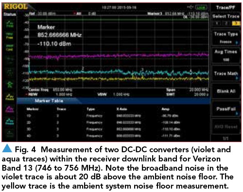
Once the various noise sources on the board are identified and characterized, the second useful measurement is to narrow the span and look at just the receiver (downlink) band using the same near field probe in various locations. For ex- ample, the downlink band for Verizon LTE in the U.S. would be “Band 13” of the FCC allocation from 746 to 756 MHz (see Figure 4). By probing all the remaining circuitry, you may be able to identify other potential interfering sources.
One may need an external broadband preamplifier with at least 20 dB of gain in order to clearly observe the noise at these higher frequencies. Alternatively, an analyzer with an internal pre-amplifier may suffice. One may need to make these measurements inside a shielded room in order to exclude other mobile phone transmissions from disrupting your measurements.
Characterize DC-DC Converter Ringing and Rise-Times
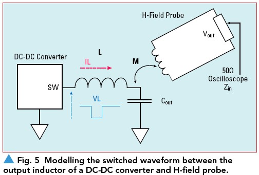
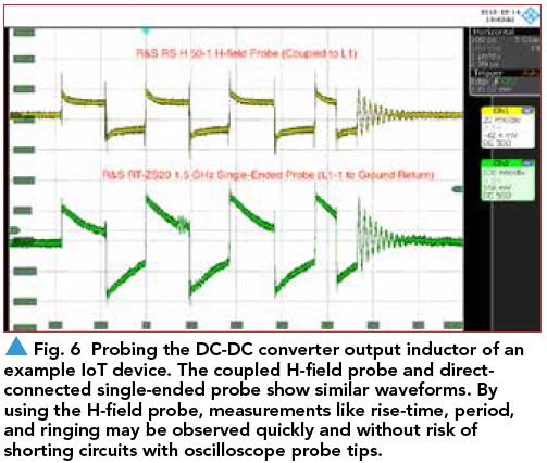
A third useful measurement using the H-field probe may be used to characterize the switching waveforms of the various DC-DC converters in the time domain. This is important for identifying ringing on the switched waveform, because this ring frequency can translate to broad peaking in the emission characteristics. Sometimes these broad peaks in emission coincide with cellular bands. H-field probes are quick and safe because they do not require direct connection to the circuitry—just couple it to the output inductor.
In order to show this is a valid characterization measurement, and referring to Figure 5, let us examine the math. There will be some unknown mutual coupling factor, M, between the inductor and H-field probe. Because we do not know the mutual coupling factor, the amplitude will not compare with actually measuring with an oscilloscope probe. However, for EMI purposes we are mainly interested in the rise-time, general switched wave shape, and ringing frequency, if any. See Figure 6 for an example comparison between the switched waveform characteristics from a Rohde & Schwarz RT-ZS20 oscilloscope probe and the RS H 50-1 H- field probe showing that the measured results are generally comparable.
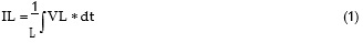
A DC-DC converter usually has a near square wave signal, VL, from the converter switch node, SW, and output inductor, L, input to ground return and this is what we would measure with an oscilloscope probe. The current through the inductor is related to that voltage as:
Assuming the H-field probe is held close to the inductor, we get some mutual coupling, M (unknown), and the output of the probe is:

Because Vout is proportional to VL, the most important characteristics for EMI are now easily and quickly measured without the risk of shorting connections with oscilloscope probe tips during circuit operation. By using the H-field probe held close to each DC-DC converter inductor, we can measure the rise-time (indicates the upper range of har- monic frequencies), pulse width and period (also factors into harmonic frequencies), and ringing frequency (which can cause broad resonant peaking in the broad band spectrum). See Figure 6 for a comparison between measuring with scope and H-field probes.

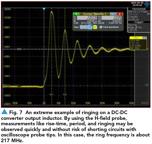
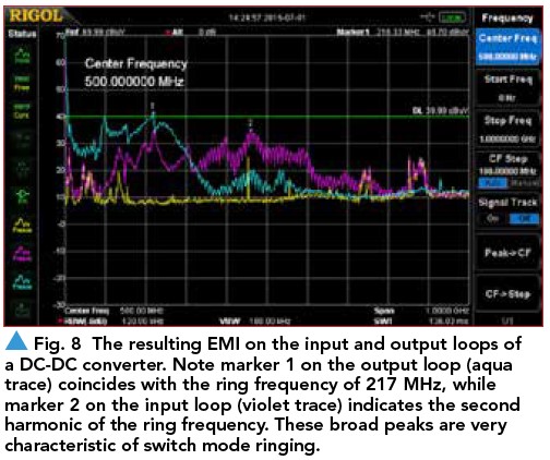
In Figure 7, we see a rather extreme example of ringing from a DC-DC converter. The ring frequency is 217 MHz and the resulting EMI peaks at this ring frequency, as well as the higher harmonics. We can see this resulting peaking in Figure 8.
Step 2: Using Current Probes
Figure 9 shows how a current probe is used to measure the common mode harmonic currents flowing along a power cable to the wildlife camera. How these currents are formed and why they tend to couple onto cables is explained more completely in references 3 and 4. Let us just assume that small RF common mode currents generated on the PC board (usually in the µA range) can easily couple to attached I/O and power cables, which can then re-radiate into the radio module as we saw modelled in Figure 1.
An oscilloscope with an FFT feature, such as the Rohde & Schwarz RTE- or RTO-series oscilloscopes or a spectrum analyzer used in Figure 9, is the most useful tool for these measurements, as entire frequency spectrums may be observed.
The current probe can measure RF common mode currents in either power cords or I/O cables. Either can radiate directly to IoT antennas.
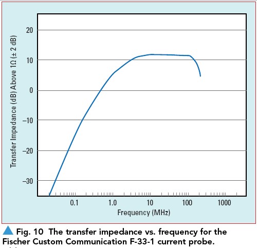
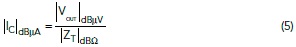
All commercial current probes, such as the Fisher F-33-1, have a calibration chart included that shows the transfer impedance (usually dBΩ) vs. frequency (see Figure 10). The nearly flat horizontal linear region is the most useful part of the plot, as you can use a constant transfer impedance to calculate the common mode current in the measured wire or cable.
To calculate the current through the probe, we use Ohm’s Law:
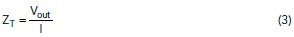
where Vout is the measured voltage at the 50Ω port and I is the common mode current in the wire or cable.
We can express this equation in dB:

Solving for I (common mode current through the wire or cable):
One very interesting outcome, is that knowing the common mode current traveling in a wire (assuming the length is electrically short compared to a wavelength), we can calculate the expected E-field from this wire or cable, based on the following equation:3-4
where Ec,max is the calculated E-field (V/m), Ic is the measured common mode current (A), f is the harmonic frequency (Hz), L is the length of the wire or cable (m), and d is the measured distance from the wire or cable (m). Typically 3 or 10 m is used for radiated emissions in order to compare with test limits in commercial EMC standards.
The ability to calculate the approximate pass or fail, given the harmonic current measurement of a wire or cable is a powerful tool when dealing with radiated emissions from a product.
While this ability is not as important when dealing with near-field emissions directly into sensitive IoT receivers, it is still nice to know, relatively speaking, whether a given power or I/O cable might be contributing to the overall noise coupling issue.
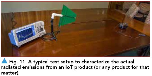
Step 3: Close-Spaced Antenna
To measure the direct emissions from a PC board with or without cables attached, you may use a close-spaced antenna to pick up the emissions. The antenna does not need to be calibrated or even resonant over the entire frequency range, just positioned at a close enough distance where harmonic emissions may be observed. The antenna may need to be positioned closer than 1m to observe the emissions from self- interference (see Figure 11).
The most important harmonic frequencies to monitor would include the cellular LTE bands (approximately 700 to 900 MHz, the commercial GPS L2 frequency of 1575.42 MHz, the higher cellular bands around 1.8 to 1.9 GHz, and the Wi-Fi ISM band of 2.4 to 2.5 GHz). On-board harmonic con- tent seldom goes higher than that.
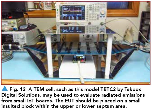
Step 3: TEM Cells (Option)
An alternative to setting up an antenna would be to use a TEM cell to characterize the emissions from a bare IoT board or IoT product, assuming it will fit within the septum area.
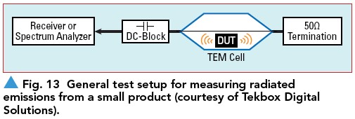
In order to measure the direct emissions from a PC board with or without cables attached, it may be placed into a small TEM cell (see Figure 12), such as the ones manufactured by Tekbox Digital Solutions.5 A TEM cell is simply an expanded 50Ω transmission line. Placing an operating test board (protected with an insulator) within the septum area can capture the general emission profile.
In use, connect a 50Ω termination to one port of the TEM cell and a DC block to the other for protection of the oscilloscope or spectrum analyzer in case DC voltage ends up on the septum plate. Then connect a coaxial cable from the DC block to the oscilloscope or analyzer input and adjust for the desired frequency limits (see Figure 13).
Because of the open TEM cell design, this test may also have to be performed in a shielded room in order to exclude strong ambient RF signals from broadcast stations, television, or cellular transmitters.
Any attached cables may pick up ambient signals from radios, televisions, 2-way radios, or cellular phones. If that is the case, try attaching several equally-spaced ferrite chokes along each cable. In any case, it is best to record an ambient plot over the frequency range being measured to help identify and distinguish between ambient and board-generated signals. If the IoT product can be powered from batteries, that is even better, as the cables may be eliminated.
Remediation Checklist
All wireless or IoT product designs must be developed with EMC/EMI in mind and any deviation may increase the risk of receiver sensitivity desense. Important considerations include:
- A near perfect PC board layout (stack-up, routing, solid return planes)
- Possibly substituting linear regulators instead of switch- ing regulators
- Use of the newer “Low-EMI” switching regulators
- Filtering of DC-DC converters
- Filtering of any other high-frequency device
- Filtering at the radio module
- Local shielding around high EMI areas, such as proces- sor/memory or DC-DC converters
- Possibly shielding the entire product (antennas excepted)
- Proper antenna placement and design
The PC board layout is critical and is where most of your effort should be spent. An 8- or 10-layer stack-up will provide the most flexibility in segregating the power supply, analog, digital, and radio sections and provide multiple ground return planes, which may be stitched together around the board edge to form a Faraday cage. Care must be taken to avoid return current contamination between sections through common impedance coupling, that is, sharing a common signal return path. That is why partitioning of circuit functions (RF, digital, analog, power conversion) is so important.
It is vital that the power and ground return planes be on adjacent layers, and a maximum of 3 to 4 mils apart. This will provide the best high-frequency decoupling. Clocks, or other high-speed traces must be adjacent to solid return planes, should avoid passing through too many vias, and should not change reference planes without adjacent return via or stitching capacitors.
On-board DC-DC power supply sections should be well isolated from sensitive analog or radio circuitry (including antennas). Be aware of primary and secondary current loop areas and their return currents. These return currents should not share the same return plane paths as digital, ana- log, or radio circuits. Typically, it is best to place the input and output capacitors, as well as the output inductor, very close to the DC-DC converter IC. Remember that return currents above about 50 kHz want to return directly under the source trace. Finally, locate all associated converter circuitry on either the top or bottom of the PC board. Placing them on both sides will cause high frequency currents to contaminate the dielectric space and could cause EMI coupling to other circuits.
For general product design guidelines, references 3 and 4 describe several basic design concepts to reduce EMI. Reference 6 includes a series of articles on designing PC boards for low EMI. Reference 7 is useful in providing ideas for measurement of wireless EMI and remediation.
Summary
Wireless self-interference has quickly become one of the most challenging issues for manufacturers developing IoT products. Success depends on carefully designing the entire product to ensure minimal self-generated EMI. Proper circuit board layout and stack-up are key factors for success.
Article was published in the SIJ July 2019 Print Issue, Technical Feature: Page 34.
References
-
CTIA, “Test Plan for Mobile Station Over the Air Performance: Method of Measurement for Radiated RF Power and Receiver Performance,” http:// files.ctia.org/pdf/CTIA_OTA_Test_Plan_Rev_3.1.pdf.
-
Broadcom, “Compliance with TIS and TRP Requirements,” www.broadcom.com/collateral/wp/21XX-WP100-R.pdf.
-
H. W. Ott, “Electromagnetic Compatibility Engineering,” Wiley, August 2009.
-
P. G. André and K. Wyatt, “EMI Troubleshooting Cookbook for Product Designers,” SciTech, July 2014.
-
Tekbox Digital Solutions, www.tekbox.com/product/open-tem-cells-emc-compliance-testing/.
-
K. Wyatt, “The EMC Blog,” EDN, www.edn.com/electronics-bCopylogs/4376432/The-EMC-Blog.
-
K. Slattery and H. Skinner, “Platform Interference in Wireless Systems— Models, Measurement, and Mitigation,” Newness Press, 2008.