
In the high-speed connector design arena, there are two opposing ideas. For some people, if you simply put pieces of plastic and metal together, eventually you have a signal transmission. This process is very simple. On the other end of the spectrum, there is the idea that a solid connector design requires a deep understanding of electromagnetic theory, a wisdom only sorcerers and wizards possess. As with almost everything in life, the truth lies somewhere in between. In this article I will try to demystify some concepts of high-speed connector design.
Opposing Views and Consideration
Let me start by stating that, “No, it is not that simple.” If it were, companies would not have dedicated teams just for connector design. On the engineering side alone, those teams are composed of signal integrity (SI) engineers, mechanical engineers, and manufacturing engineers. If SI engineers talk about impedance, crosstalk, and insertion loss (fun stuff), mechanical engineers talk about normal force or mating cycles (boring stuff), and the manufacturing engineers talk about tooling or molding (even more boring). And I am not even considering the business side, as engineers usually do not care too much about the cost: “Who cares if it is too expensive? It is a beautiful design!” As you can see, high-speed connector design is a multi-disciplinary endeavor and is not as simple as putting metal and plastic together.
On the other hand, some SI engineers make the electrical part of the connector design sound like sorcery. When there is a problem with some squiggly lines, we, the SI-wizards, can make them go up, down, appear, and disappear! It might take some experience and knowledge, but it is certainly not magic. In this article, I will explore what we do in the SI side of the connector design.
Electrical Side of a High-speed Connector Design
There are several different parameters that must be addressed when dealing with high-speed design. Those would include crosstalk, losses, impedance, common mode, mode conversion, coupling, and the like, and there will never be agreement on what to be considered first, and what is more or less relevant. Ultimately, it boils down to what the customer needs. Here, I will focus on the two aspects that I spend most of my time on when designing high-speed connectors: differential impedance (return loss) and resonances (insertion loss).
Because high-speed connector design is not trivial, we can understand why most companies are very protective of their designs. It would be difficult to convince any organization involved in that market to share their intellectual property, but we can gather some insights about what is relevant and address the issues with a simple board. For example, a differential microstrip with coplanar ground and some ground stitching vias between the top ground pour and bottom ground layer is a good test vehicle to illustrate these design principles.
Impedance
If the cross-section profile does not change along the propagation direction, the differential impedance does not change either. However, sometimes the ground plane is cut underneath the signal trace, bringing the impedance up. Or the stitching vias come too close to the signal trace, or the two signal traces are too close together, bringing the impedance down. Figure 1 illustrates these phenomena.

Fig. 1 Differential impedance profile for a differential microstrip trace. Impedance goes up where there is a ground plane cut, and it goes down where the traces are wider (closer).
This is how we tune the impedance when designing a connector: if we want the impedance to go down, we add metal or bring the traces (or the ground) closer together. If we want it to go up, we remove metal or pull traces or ground further apart. In the example shown here, things would be easy, as we would simply try to make the cross-section constant. In a real connector design, things would be more involved. We would tune the differential impedance until we reached the flattest possible profile. A detailed analysis on how impedance is calculated, and the difference between single-ended and differential modes, was recently done.1
Resonances
Once impedance is at its best, we can turn our attention to resonances. They will appear in the insertion loss profile, and they usually carry over to return loss and crosstalk. There are two types of resonances to be addressed: one that is caused by stubs in the signal path and one that is caused by the return path or the ground structure.
The first one has been explained by several experts in the industry2, 3 with via stubs in the board. In connector design, that phenomenon also occurs and is related to the wipe between the two mating pins. Even though the geometry is mechanically different, from an electrical perspective it is the same: if you allow the signal to travel between the contact point and a short at the end of the wipe or the via, it will create a resonance proportional to the length of that stub. Figure 2 illustrates the parallel between via stubs and connector mating stubs. In an ideal electrical design, no wipe is allowed in the connector so no stub is present. But mechanically that is not possible, and a compromise between electrical performance and mechanical reliability has to be achieved. The longer the wipe, the lower the frequency the connector will resonate. This is one difference between a 1 GHz connector and a 40 GHz connector: a 40 GHz connector cannot afford a long wipe the same way a board for 40 GHz performance will have to include backdrilling to remove via stubs.
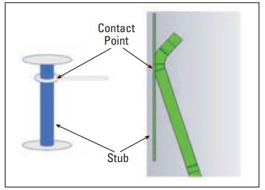
Fig. 2 Stub effect in both a via and a connector mating point.
Even if the signal path is perfect, there may still be resonances. The return path is the name of the game here. The distance between the stitching vias will determine the frequencies where the resonances in the plane-to-plane structures will occur. This is another difference when designing a connector to perform at 1 GHz versus a connector to perform at 40 GHz: the higher the frequency the connector is supposed to work, the shorter the relevant return path structures must be.
If, for example, the connector has ground pins, they will have to be stitched in such a way as to push the resonance beyond the minimum desired frequency. Once again, we use the microstrip example to illustrate this concept. Figure 3 shows this phenomenon. The closer the stitching vias are, the higher the resonant frequency of the top and bottom ground-plane-cavity.
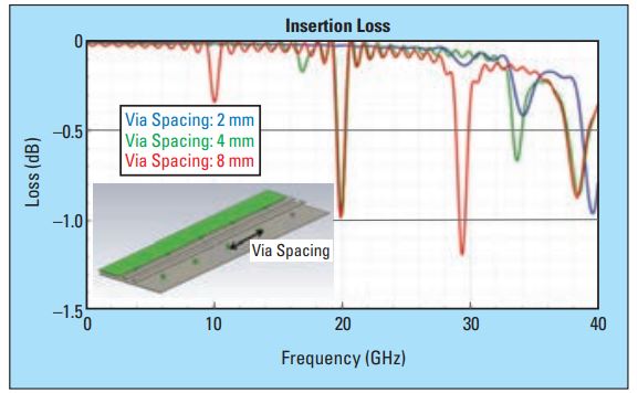
Fig. 3 Insertion loss as a function of the via space.
It may be tempting to believe everything is clear now. Not so fast… Notice in Figure 3 that the resonant frequencies for the 8 mm via spacing example happen in multiples of 10 GHz, but there are also different combinations at different frequencies when you look at the 4 mm via spacing example.
For example, there are some problems at 17 GHz and 34 GHz. The reason is that the distance between the stitching vias can be measured along the direction of the top ground strip (like we are doing) but also across the top ground strip. The latter could be the dominant effect in some cases. Or even a combination of the two could be responsible for the ground-plane-cavity resonance.
Keep in mind that this is a very simple microstrip trace. In a real-life connector design, things are not so straightforward. One way of determining where the problem is, is to look at the fields at the resonant frequency. My colleagues and I have taken a deeper look into this problem in the past.4 Figure 4 highlights the concept behind this approach.

Fig. 4 Basic electromagnetic theory used for resonant cavity problems.
Essentially, we turned our attention to the principle of resonances and asked the question, “Where do they originate?” From fundamental electromagnetic theory, resonances occur when you have a cavity and the electromagnetic fields are trapped inside such cavity. Notice that the modes (possible solutions) can be a function of x, y, or z, and the dominant mode will depend on the cavity dimensions. Similarly, in our microstrip trace example, the resonant frequencies of the top plane to bottom plane cavity can be a function of the via spacing in the x-direction, in the y-direction, or a combination of both, and it is not always obvious, especially when designing a connector, where the problem might be.
To expand on the basic theory, we substitute the idealized cavity with a connector-like geometry. This is accomplished by using an eigenmode solver to identify the frequencies where resonances can occur. Not only is the eigenmode solution significantly faster than a full frequency sweep, but once a solution is available, the field plots are also available. This allows the user to see the areas where the resonance is strongest, helping the engineer tackle the problem from a theoretical and fundamental point of view, as opposed to trial-and-error.
The eigenmode solution is obtained with the ground structure alone by removing the signal pins, thus allowing the ground structure to be treated as a resonant cavity like the basic cavity described in Figure 4. In addition to providing a list of possible resonant frequencies, the eigensolver also provides the Q factor associated with each resonant mode. The Q factor indicates how strong a mode will resonate if excited. The higher the Q value, the stronger the resonance for that mode.
We simulate a common geometry found in high-speed connectors. This geometry is composed of four wafers (metal pins embedded in plastic). The inner signal wafers, which constitute a differential pair, are sandwiched between two ground wafers, as shown in Figure 5.
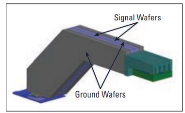
Fig. 5 High speed connector example.
In the first structure, there was an air gap between the signal wafers and the ground wafers, as shown in Figure 6. This is referred to as the gap structure (GS).
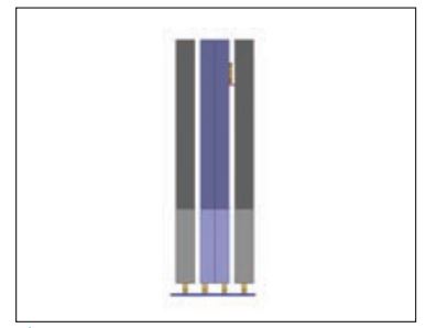
Fig. 6 Cross section, with ground-signal (GS) Gap.
This structure was analyzed using an eigenmode solver. Table 1 summarizes the resonant frequencies and their associated Q values.

This same geometry was also analyzed in the frequency domain with a full frequency sweep. In general, a full sweep over the entire frequency range of interest is at least one order of magnitude slower than the eigenmode solution. The corresponding insertion loss curve for this structure is shown in Figure 7.
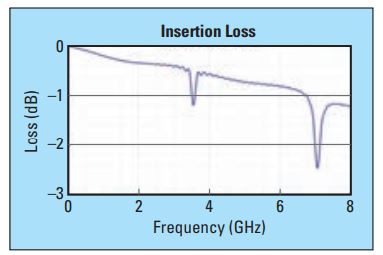
Fig. 7 Insertion loss plot for GS Gap structure shown in Figure 6.
Notice that the resonances in Figure 7 align with Modes 1 and 5 in Table 1. Eigenmode solutions determine all frequencies at which a given structure may resonate, but not all modes will be excited by the differential signal. For cases where the differential eigenmode is not obvious, the user may look at the full 3D field distribution of the eigenmode solution.
Instead of spending the computation time to do the frequency sweep, a more efficient way to investigate which eigenmodes are of relevance is to look at the eigenmode field plots. This method is at least one order of magnitude faster than a traditional full sweep. By examining the fields, the user can discern which ones are generated by a differential signal.
Figure 8 shows eigenmode field plots that identify a resonance likely to occur with a differential energy (left) and an eigenmode field that is not likely to be excited by differential energy (right). Often, the first eigenmode (at 3.5 GHz in this example) is the one relevant to a differential mode, which is of primary concern. Additionally, higher order harmonics (e.g. Mode 5 at 6.9 GHz) are also usually relevant.
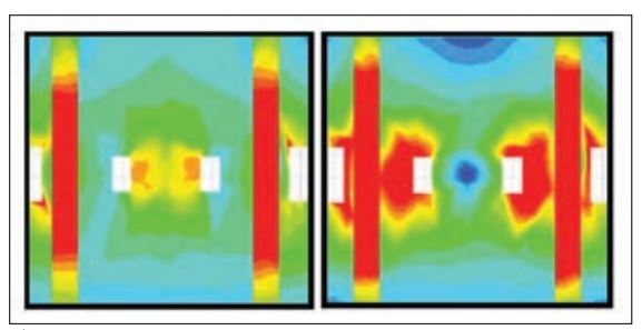
Fig. 8 Electric field distributions showing a mode excited by differential energy (left) and a mode not excited by differential energy (right).
Returning to the GS Gap structure, the performance may be improved by reducing the strength of the resonances. In other words, the geometry may be tuned such that the resonant modes yield lower Q factors. One way this is accomplished with this geometry is by reducing the GS air gap, as shown in Figure 9. The results of the eigensolver are summarized in Table 2.

Fig. 9 Cross section, with reduced GS Gap.

The reduction in Q factor is apparent comparing the results in Tables 1 and 2, particularly for Modes 1 and 5. Therefore, the reduced GS Gap geometry is expected to perform better. Indeed, when a full frequency sweep is simulated, the insertion loss curve showed a significant improvement, as shown in Figure 10.
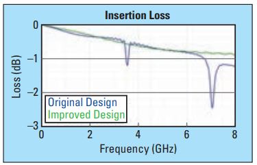
Fig. 10 The reduction in Q factor translates into better insertion loss curve.
Finally, as we saw previously, adding or removing metal in a connector will have an impact on the impedance. Changing the location of the wafers also impacts the impedance. In most cases, the designer will have to revisit the impedance tuning before reaching an optimal electrical performance.
Conclusion
In the ideal SI world, we would just tune impedance, add more ground connections wherever we see fit and call it a day. But one cannot simply ignore everything that goes around the connector. Usually, we would go back-and-forth between SI, mechanical, and manufacturing. At every step we make sure at least impedance and insertion loss perform as expected. And I am fully aware that I am not even talking about all the other SI metrics that can come into play, like common mode, crosstalk, mode conversion/skew, etc.
To bring it all home: no, high-speed connector design is not just plastic and metal stitched together. It is not magic either. It does take some experience and knowledge, but some things can be explained in simple terms. And some others are a bit more advanced. n
Acknowledgment
At the time of writing this article, Davi Correia was with Carlisle Interconnect Technologies. He has recently changed affiliations and is now with Cadence Design Systems.
References
1. Bert Simonovich, “What is Differential Impedance and Why do We Care?” Signal Integrity Journal, 14 April 2020. https://www.signalintegrityjournal.com/blogs/12-fundamentals/post/1665-what-is-differential-impedance-and-why-do-we-care.
2. Bert Simonovich, “Via Stubs – Are They all Bad?” Signal Integrity Journal, 10 March 2017. https://www.signalintegrityjournal.com/blogs/7-voice-of-the-experts-signal-integrity/post/355-via-stubs-are-they-all-bad.
3. Eric Bogatin, “How Long a Stub is Too Long,” EDN, 23 October 2014, https://www.edn.com/how-long-a-stub-is-too-long-rule-of-thumb-18/.
4. Davi Correia, Michael Rowlands, and Alexandra Haser, “GSSG Resonance Method for Interconnect Designs,” Signal Integrity Journal, 7 June 2017, https://www.signalintegrityjournal.com/articles/441-gssg-resonance-method-for-interconnect-designs.
Article was published in the SIJ July 2020 Print Issue, Cover Feature: Page 8.