
Coping with SI (signal integrity) and EMI (electromagnetic interference) issues is a daily challenge for PCB design engineers. While many rely on design reviews and manual checking to identify these issues, a more efficient way to pinpoint them is the use of automated design rule checks (DRCs). These DRCs can be programmed and customized to identify common SI and EMI issues much faster and more reliably than manual inspection. This article discusses some of the common SI and EMI issues that can be found using DRCs.
COMMON CAUSES OF EMI IN PCBs
The most common cause of radiation from a PCB is a deviation or break in the return current path for a signal. Any time a high-frequency signal does not flow in a closed loop, an antenna is created, whether intentional or not. On a PCB, part of that loop is created by electromagnetic fields coupled between the signal trace and it reference plane, and any break in that path will create an antenna and cause radiated emissions.
- NET CROSSING A GAP
The most severe case of a broken return path is a signal net crossing a gap in a reference plane (see Figure 1). When a signal net crosses a plane split, the return path is completely broken, and current will need to traverse an alternate path (usually made by some capacitance on the board) to form a closed loop. The wider the deviation, the more high-frequency content is radiated as EMI. This problem can be somewhat mitigated by placing a stitching capacitor close to the crossing, but because a mounted capacitor is a narrowband structure, it does not completely eliminate the problem.
Another, less severe instance of this is when the signal net crosses a hole or slot in the reference plane. In this case, the deviation in return current is much smaller, but some radiation will occur, more-so for larger slots.
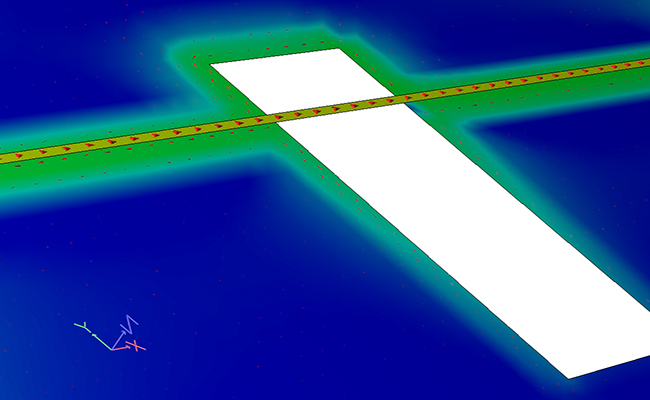
Figure 1. Deviation of return current for trace crossing a slot in the reference plane (shown in HyperLynx 3D)
- VERTICAL REFERENCE PLANE CHANGE
An equally common occurrence on a PCB is a signal changing references as it passes through a via. This can cause a break in the return path if the different reference planes are not connected together. This is usually done with a stitching via, but if the planes are different voltages, then the stitching must be done using a capacitor, or group of capacitors. Also, if a signal is not referenced to its own voltage, i.e. the voltage that is used to power its I/O buffers, then there will be another less obvious break in the return path.
- NET NEAR A PLANE EDGE
A somewhat less severe cause of radiation is when a signal net is routed close to the edge of a reference plane. This causes a perturbation in the electromagnetic field coupling that can cause some of the energy to be radiated instead of being coupled to the reference plane. An easy way to avoid this is to ensure signals stay a minimum distance away from the edge of the plane.
COMMON CAUSES OF SI ISSUES IN PCBS
Ensuring signal integrity on today’s modern PCBs can often be quite complicated, and require elaborate simulations to validate performance. However, some of the basic necessities for signal integrity on a net can be validated using DRCs.
- IMPEDANCE
One of the most basic elements to ensuring proper signal integrity on a bus is making sure the signal traces have the correct impedance. This is determined by the trace geometries – width, thickness, and height above the reference plane – as well as the board material properties, specifically the dielectric constant. In a real design, other factors can affect the trace impedance, like holes in the reference planes, proximity to area fills, or neckdowns in IC or connector pinfields. Validating the correct impedance along the entire trace route can be complicated, but is essential to minimizing reflections and ensuring maximum margin.
- DIFFERENTIAL IMPEDANCE
The same concerns affect differential pairs as well, and actually become more crucial because differential pairs typically have faster signal edges and run at lower voltages, so there is much less margin for any unnecessary reflections on the bus. Because differential pairs consist of a pair of traces, in addition to the other factors, the spacing between the traces is an additional concern. Trying to maintain that spacing throughout the board can be difficult but is vital.
- VIA STUBS
Another common problem for high-speed differential signals is the presence of stubs on signal vias. For a normal thru-hole via, unless the signal transitions from the top of the board to the bottom, there will be some amount of the via that is acting like a stub. This will add additional unwanted reflections, some significant enough to distort the received signal beyond recognition. Techniques like backdrilling and the use of blind/buried vias can reduce or eliminate via stubs, at an additional cost. Careful layer section can also keep stubs to a minimum, but must be ensured for every multi-Gb signal.
- CROSSTALK COUPLING
Any time two traces are routed parallel to one another there will be energy coupled between them. This coupling will be less the further apart the traces are, and the shorter the length of parallelism. While knowing the exact effect crosstalk will have on a received signal is more complicated, knowing the amount of coupled voltage is more straightforward and can be calculated using the trace geometries and the voltage and edge rate of the signals. Designs can be checked to highlight any areas of excessive crosstalk coupling.
DRCs
Running DRCs is an excellent complement to simulation for ensuring signal integrity and electromagnetic compatibility on a high-speed PCB design. The mitigation of EMI is a great example of this; someone can run hours of simulations in a 3D field solver to determine radiation strength of a net crossing a gap in the reference plane, or knowing this is an obvious problem, run a DRC on the design in a matter of minutes to identify any gap crossings so they can be eliminated. Insight into specific design types or busses that is gained from simulation can also be programmed into DRCs, so that similar designs can be verified to have the same performance.
This type of design expertise or IP becomes much more leveraged when encapsulated in a DRC. In addition, the use of DRCs allows design reviews to be performed much faster, and in a manner that is repeatable across multiple designs.
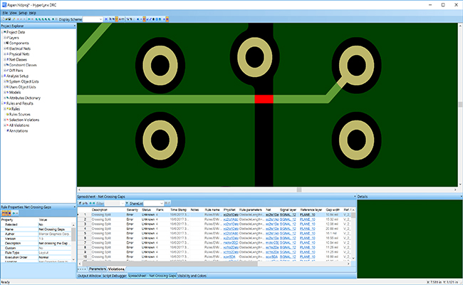
Figure 2: Net Crossing Gap Violations Detected in HyperLynx DRC
Utilizing DRCs to automatically identify potential SI and EMI issues on PCBs provides greater confidence in the PCB design, dramatically increasing the probability for first-time success and reducing the number of design revisions.
SUMMARY
EMI and SI issues simply cannot be ignored in modern high-speed PCB designs. Many of these issues are simple and/or well-known, so using DRCs is especially effective in helping eliminate these issues. The design process can often bring about unexpected design issues, in addition to expected ones, so design reviews are essential. Making those design reviews accurate, complete, repeatable and efficient can all be accomplished by using DRCs.
Author's Biography
Patrick Carrier is the engineering planning manager for the Mentor Board Systems Division. He has more than 17 years of experience in the field of signal and power integrity and previously worked as a signal integrity engineer at Dell before joining Mentor in 2005, supporting the HyperLynx high-speed PCB analysis tools. He has written dozens of technical articles and is a recognized speaker at technical conferences.