
In the design of high-speed connectors, one of the main issues faced by the designer is the appearance of resonant frequencies. If a connector resonates at a particular frequency, that frequency will not be transmitted through the channel, reducing the quality of the signal at the receiving end and potentially compromising the entire link. The problem is particularly relevant if those resonant frequencies happen to be close to the Nyquist frequency of the desired data transfer rate. For many interconnect products, more than 50% of design time is spent on reducing resonances. The baseline structure and impedance tuning are usually fast, but the resonance reduction effort takes a long time. This paper provides a basic electromagnetic understanding of resonant behavior, a method for quickly determining resonant frequencies, a secondary set of metrics to evaluate if a particular frequency is excited or not, a set of examples and a conclusion. The goal is to help the signal integrity community to understand and address the issues using a systematic approach, by identifying the root-cause of the problem and proposing different ways to solve it.
Electromagnetic Theory- Resonant Frequencies
In order to address the resonant problem, we will start by approximating a real connector geometry by a resonant cavity. Suppose we have a cavity with an open boundary condition on the top and on the bottom. We will approximate that by a perfect magnetic conductor (PMC), where the tangential magnetic field is zero. Likewise, the remaining four faces will be approximated by a short or a perfect electric conductor (PEC) boundary condition, where the tangential electric field is zero [1]. Moreover, assume the dimensions of our cavity are a, b, and c, like shown in Figure 1. This assumption is a reasonable approximation of a ground structure of a connector. The signal pins are surrounded on two sides by ground pins, which are terminated (shorted) at either end of the interconnect. For the resonant cavity, the signal pins will not be included, only the ground structure. This leaves two sides of the signal pair exposed (open). It should be noted that the theory developed here does not rely on any particular boundary condition assumption.
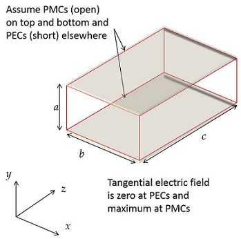
Figure 1 Resonant cavity geometry
If the assumption on the boundary condition is followed, the possible solutions for Maxwell’s equations with the given boundary conditions are given by [1,2]
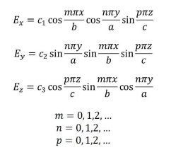
where p and n cannot be zero at the same time, cn are constants that relates electric and magnetic fields and Ex, Ey, Ez, are the electric field components in x, y and z directions, respectively.
Another important feature of the resonant cavity modes is that each particular mode exists at one particular frequency. This frequency is known as the resonant frequency of that mode and is given by
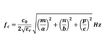
where c0 is the speed of light in the vacuum and ɛr is the dielectric constant. One particular mode that we will be interested in is the mode known as TE001. The field distribution for this mode is shown below in figure 2. Its resonant frequency is given by fc=c0/(2a sqrt(ɛr))
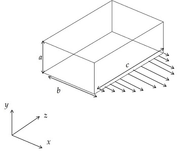
Figure 2 Electric field distribution for mode TE001 inside the cavity.
This mode is particularly important for two reasons: it has the lowest cutoff frequency of all modes and can usually be excited by most connector geometries.
Eigenmode Solution
The ultimate objective of any EM solver is to accurately solve Maxwell’s equations. However, a sweep over a band of frequencies is computationally expensive and is therefore time consuming. Conversely, time-domain solvers solve the entire frequency band in a single run, but they might suffer inaccuracies if the geometry is complex or it is computationally expensive if the problem has a large number of ports.
Another approach is to expand on the theory developed in the first section, substituting an idealized cavity with a particular connector geometry. This is accomplished by using an eigenmode solver to identify the frequencies where resonances are able to occur. Not only is the eigenmode solution significantly faster than a full frequency sweep, but, once a solution is available, the field plots are also available. This allows the user to see the areas where the resonance is strongest, helping the engineer tackle the problem from a theoretical and fundamental point of view, as opposed to trial-and-error. The eigenmode solution is obtained with the ground structure alone by removing the signals pins, thus allowing the ground structure to be treated as a resonant cavity like the one previously described. In addition to providing a list of possible resonant frequencies, the eigen solve also provides the Q factor associated with each resonant mode. The Q factor indicates how strong a particular mode will resonate if excited. The higher the Q value, the stronger the resonance for that particular mode. (All simulations presented in this paper were done using ANSYS HFSS solver.)
Example Eigenmode Solution
In our first example, we simulate a common geometry found in high-speed connectors. This geometry is composed of four wafers (metal pins embedded in plastic). The inner signal wafers, which constitute a differential pair, are sandwiched between two ground wafers, as shown in Figure 3.
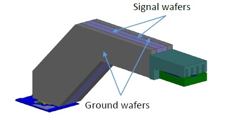
Figure 3 High speed connector example.
In the first structure, there was an air gap between the signal wafers and the ground wafers, as shown in Figure 4. This is referred to as the GS Gap structure.
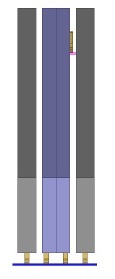
Figure 4 Cross section, with ground-signal (GS) gap.
We analyzed this structure using an eigenmode solver. It took approximately 7 minutes for HFSS to obtain the solution. Table 1 summarizes the resonant frequencies and their associated Q values.
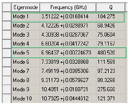
Table 1. Eigen mode solutions for GS Gap structure.
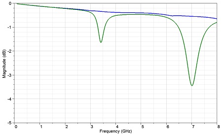
This same geometry was also analyzed in the frequency domain with a full frequency sweep. It took approximately 70 minutes for HFSS to converge to the solution. The corresponding insertion loss curve for this particular structure is shown in Figure 5.
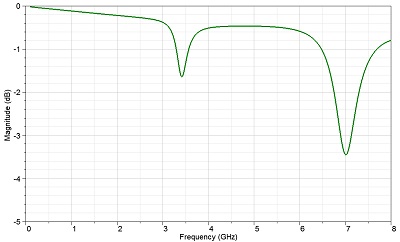
Figure 5 Insertion Loss plot for GS Gap structure shown in Figure 4.
Notice that the resonances in Figure 5 align with Modes 1 and 5 in Table 1. Eigen solves determine all frequencies at which a given structure may resonate, but not all modes are differential. For cases where the differential eigenmode is not obvious, the user may look at the full 3D s-parameter results, or look at eigenmode fields. For instance, the insertion loss results in Figure 5 show a resonance that matches the first eigenmode in Table 1.
Instead of spending the computation time to do the frequency sweep (~70 minutes to solve), a more efficient way to investigate which eigenmodes are of relevance is to look at the eigenmode field plots (~7minutes to solve). The proposed method is one order of magnitude faster than a traditional full sweep. Besides, by examining the fields, the user can discern which ones are generated by a differential signal. Figure 6 shows an eigenmode field plot which identifies a resonance likely to occur with a differential energy (left) and an eigenmode field that is not likely to be excited by differential energy (right). Often, the first eigenmode (at 3.5 GHz in this example) is the one relevant to a differential mode, which is of primary concern. Additionally, higher order harmonics (e.g. Mode 5 at 6.9 GHz) are usually relevant as well.
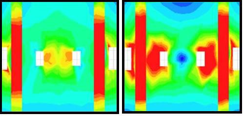
Figure 6 Electric fields distribution showing mode excited by differential energy (left) and mode not excited by differential energy (right).
Returning to the GS Gap structure, the performance may be improved by reducing the strength of the resonances. In other words, the geometry may be tuned such that the resonant modes yield lower Q factors. One way that is accomplished with this geometry is by reducing the GS gap, as shown in Figure 7. The results of the eigen solve are summarized in Table 2.
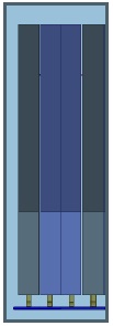
Figure 7 Cross section, with reduced ground-signal gap.
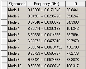
Table 2. Eigen mode solutions with reduced GS gap.
The reduction in Q factor is apparent comparing the results in Tables 1 and 2, particularly for Modes 1 and 5. Therefore, the reduced GS Gap geometry is expected to perform better. Indeed, when a full frequency sweep is simulated, the insertion loss curve showed a significant improvement, as shown in Figure 8.
| Figure 8 . The reduction in Q factor translates into better insertion loss curve. |
Secondary Metrics
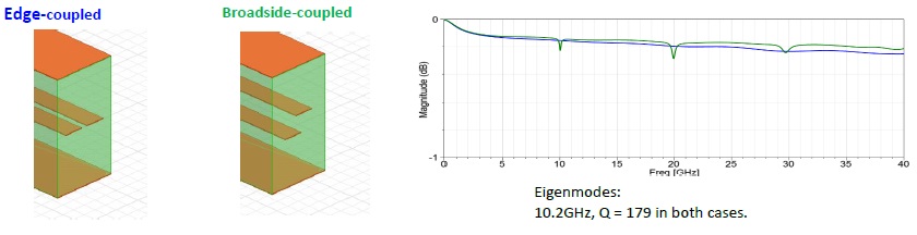
In some cases, the Q factor obtained from the eigenmode solution is not enough to explain some of the resonant behavior. For example, when an edge-coupled differential stripline is used, no resonance is observed. However, if a broadside-coupled stripline is used, resonant behavior is present. Since both examples have exactly the same ground structure, we expect the same Q factor. But their resonant profile is different. Figure 9 shows this effect.
|
Different s-parameter results with the same eigenmodes happen because the eigenmode solve only takes the ground structure into account and yields all possible modes. Whether the modes are excited is determined by the signal pin configuration and the source energy. A mode is more likely to be excited if more energy is coupled into the ground structure, or if the field distribution around the signal pins is asymmetric at a particular resonant frequency. For this analysis, the differential energy is analyzed with respect to the signal pins to determine if the mode is likely to be excited.
In order to account for the differences in the signal configuration, a set of secondary metrics is proposed. They are designed to behave similarly to Q factor in that higher values indicate stronger resonances. In the ideal resonance-reduction case, if the metric is 0, there is no resonance excited, no matter how high the Q value of the structure.
We calculated the characteristic impedance matrix using an open waveport with no ground metal. All metal in the waveport is solved as a terminal. In our example, the two ground terminals are assigned to terminals 1 and 4, while terminals 2 and 3 are the signal pins. The outer edge of the waveport shape is automatically grounded, so care must be taken on the ports. The waveport edges are placed far away from the metal to avoid disrupting the fields on the terminals, but not so far away as to create unwanted higher-order modes. Below is an example of the edge-coupled and broadside-coupled ports and characteristic impedance matrices. Tables 3 and 4 show their impedance matrices, used to obtain their corresponding secondary metrics. The ground coupling metric, is defined as GC=Z12/Z23.
This accounts for how much energy is coupled to the ground structure and hence how much energy is excited in the resonant cavity. Again, zero is the “best” value, meaning that no energy couples to the ground. A value of infinity is the “worst” case, meaning that 100% of the signal energy couples to the ground structure.
The second metric is ground asymmetry, GA= (Z12- Z13+Z43-Z42)/ (Z21+ Z31). Please note that for edge-coupled stripline, GA=0 (best-case) whereas for broadside-coupled GA≠0. In this metric, the worst-case value is 1, which means that all the energy couples to one part of the ground structure, and zero energy to the other part of the ground.
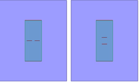
Figure 10 Port snapshots: edge-coupled (LEFT) vs. broadside-coupled (RIGHT)
|
Broadside-coupled |
1-G1 |
2-S1 |
3-S2 |
4-G2 |
|
1-G1 |
97.2 |
42.1 |
31.4 |
15.6 |
|
2-S1 |
42.1 |
121.0 |
69.8 |
31.3 |
|
3-S2 |
31.3 |
69.8 |
120.7 |
42.0 |
|
4-G2 |
15.6 |
31.3 |
42.0 |
97.2 |
Table 3. Impedance matrix used to obtain secondary metrics for broad-size coupled stripline.
Ground Coupling: GC=Z12/Z23
Ground asymmetry: GA= (Z12- Z13+Z43-Z42)/ (Z21+ Z31)
GC_broadside = 42.1/69.8 = 0.60
GA_broadside = (42.1 - 31.4 + 42.0 – 31.3) / (42.1 + 31.3) = 0.29
|
Edge-coupled |
1-G1 |
2-S1 |
3-S2 |
4-G2 |
|
1-G1 |
97.0 |
36.2 |
36.2 |
15.7 |
|
2-S1 |
36.2 |
123.4 |
70.1 |
36.2 |
|
3-S2 |
36.2 |
70.1 |
123.3 |
36.2 |
|
4-G2 |
15.7 |
36.2 |
36.2 |
97.1 |
Table 4. Impedance matrix used to obtain secondary metrics for edge coupled stripline.
GC_edge = 36.2/70.1 = 0.51
GA_edge = (36.2 – 36.2 + 36.2 – 36.2) / (36.2 + 36.2) = 0.0
The Q values of the eigenmodes are identical between the edge-coupled and broadside coupled. However, the edge-coupled has lower energy coupling to ground, and it has perfect symmetry, exactly zero asymmetry. Therefore, the edge-coupled case does not excite the eigenmode, while the broadside coupled case strongly excites the eigenmode.
Example for secondary metrics
For the example of the secondary metrics, we will revisit the example in the previous session. Starting with the structure with the reduced GS Gap, we will now add a gap between the two signal wafers, as shown in Figure 11. This geometry is referred to as the SS Gap structure.
Figure 11 Cross section, signal-signal gap.
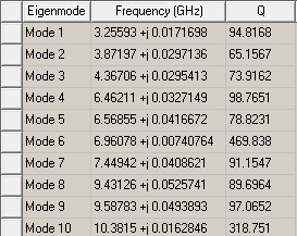
Table 5. Eigen mode solutions for SS gap.
Table 6 summarizes the Q factors and secondary metric values for the Reduced GS Gap and the SS Gap geometries. The degradation in Q factor is not as significant as in the previous example. However, if we look at the secondary metrics, we might be able to identify which structure will perform better.Table 5. Eigen mode solutions for SS gap.
|
Secondary Metric |
Reduced GS Gap |
SS Gap |
|
Q factor (Mode 1) |
90.84 |
94.82 |
|
Q factor (Mode 5) |
78.71 |
78.82 |
|
GC |
0.59 |
0.68 |
|
GA |
0.86 |
0.97 |
Table 6. Comparison between the secondary metrics for the structures shown in Figure 7 and Figure 11.
As we can see from Table 6, the secondary metrics degraded significantly by adding the air gap between the two signal pins. Even though the Q factor is both structures is comparable, we should expect the SS gap to perform much worse, as more energy will be coupled to the resonant structure. Figure 12 shows the insertion loss plot for both cases.
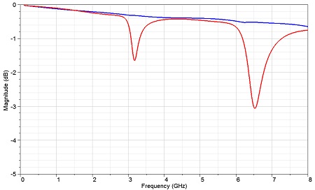
| Figure 12 Secondary metrics also explain resonant behavior. |
As expected, the SS gap structure performs significantly worse, even though the change in the Q factor is not substantial (from 90.8 to 94.8 for Mode 1). The secondary metrics also explain why an edge-coupled differential stripline doe not show the same resonant behavior as a broadside-coupled stripline: even though they both share the same Q factor, the asymmetry in the broadside-coupled excites the resonant more efficiently, degrading the frequency-domain performance.
Conclusion
In this paper we presented an efficient way of determining resonances when designing high-speed interconnects. We replaced a trial-and-error and time-consuming approach of the full frequency sweep with a faster, physics-based approach, where the resonant modes are known beforehand. Our approach is at least one order of magnitude faster than the previous one, while providing the engineer with a better physical insight of the problem. Moreover, we provided a secondary set of metrics to better identify which modes will be excited. For future research, a more detailed analysis of the secondary metrics could be performed, possibly by combining them into a single metric. Also, other domains aside from connectors could benefit from the approach proposed here.
References
[1] Balanis, C. A. Advanced Engineering Electromagnetics, John Wiley and Sons, 1989
[2] Pozar, D. M. Microwave Engineering, 2nd Edition, John Wiley and Sons, 1998