
As I/O data rates are pushed beyond 20 Gbps, the process variation of the PCB material property directly affects SERDES margin, thus impacting the overall system quality. The established extraction methodologies of the material property mostly focus on the pass/fail decision, not for monitoring and improving the process control. The goal of the suggested methodology in this paper are twofold: (1) monitoring the material variations with the minimal measurement cost/time and (2) guiding vendors to adjust the manufacturing process based on the monitored statistics.
The main objective of this work was to develop a space-efficient method that is accurate up to medium high frequency with high testing throughput while being cost effective using almost all existing testing infrastructures in a high volume PCB manufacturing environment. To meet the goal, a new Gamma-T approach utilizes the time or frequency-domain measurements for two transmission line segments and T-resonator with minimal number of cross-sectioning. Two versions of Gamma-T technique are described in this paper: the cost-effective one for the production floor and the precise one for material identification/validation in a lab environment. Both versions are suitable for the material model identification for EDA tools.
Sensitivity of both versions to the strip width variations and launch reflections is investigated. It is shown that the cost-effective technique is sufficiently robust and accurate up to 20 GHz. The precise version can be used for material identification up to 50 GHz. The key to success in this project was using the right hardware (Introbotix probes) and software. Simbeor software was used to design test fixtures, extract Gamma from TDTs and S-parameter measurements and for the material model identification with the field solver models. Our conclusion is that the technique is ready for industrial use or standardization.
The entire paper explains the specifics of the technique, explaining the sensitivity to strip width as well as launch reflections. Finally, practical examples such as those in the figures below are explained and shown.
Download the Entire paper in PDF form.
Practical examples
To test the proposed Gamma-T technique, a number of test boards were designed and investigated. One of the test boards with launches designed for the Introbotix hand-held probes is shown in Fig. 8.1. The board stackup is similar to what is expected in the production environment. Optimization of launch and vias took about 2 hours of setup and analysis time in Simbeor electromagnetic signal integrity software [16].
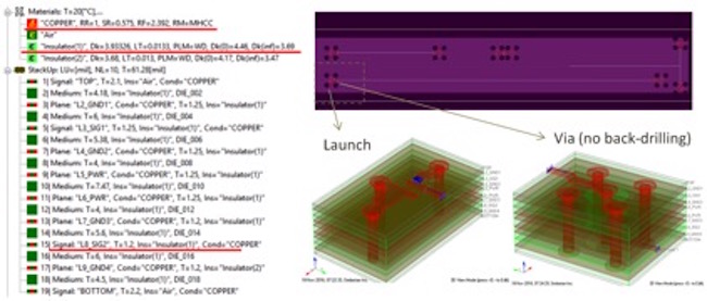
Fig. 8.1. Test board for Introbotix hand-held probes. Launch is optimized for the probe footprint for single-ended transmission line. Viahole transition from the microstrip to the strip line is optimized separately.
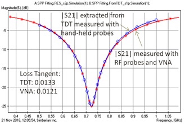
Fig. 8.2. Insertion loss of the T-resonator measured with RF probes and VNA (red curve with *) and with hand-held probes and TDR scope (blue curve with o).
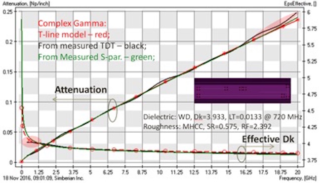
Fig. 8.3. Gamma as attenuation and phase delay extracted from TDTs measured with hand-held probes (black lines) and from S-parameters measured with VNA and probe station. Identified Wideband Debye model: Dk=3.933, LT=0.0133 @ 720 MHz. Identified conductor roughness Modified Hammerstad model: SR=0.575, RF=2.392.
The loss tangent was first identified with the T-resonator. The results are illustrated in Fig. 8.2. The resonance frequency is about 720 MHz. With the hand-held probes and TDR scope first the loss tangent is identified as 0.0133. To validate the results obtained with the TDT, we used RF probes and VNA and obtained LT=0.0121, that is within 10%. The insertion losses measured with VNA and TDR scope are very close as also shown in Fig. 8.2.
Next, Gamma was extracted from TDT measurements for two transmission lines and used to identify Wideband Debye dielectric model Dk at 720 MHz by matching computed and measured effective dielectric constant as illustrated in Fig. 8.3. Finally, conductor roughness model parameters are identified by matching the measured and computed transmission line attenuation as illustrated in Fig. 8.3. The low and high frequency defects are simply smoothed out by the frequency continuous dielectric and conductor roughness models used in the field solver. Simbeor SFS quasi-static field solver was used for the dielectric and conductor roughness model identification. The models are re-usable in other quasi-static and electromagnetic solvers. To validate the results of the cost-effective technique, the same structures were investigated with the S-parameters measured with RF probes and VNA. Gamma extracted from the S-parameters with the precise technique is shown in Fig. 8.3 for comparison. Very good correlation of the extracted Gamma with the transmission line with the identified material models can be observed.
Download the Entire paper in PDF form.
This paper was presented at DesignCon 2017.