

Introduction
In this installment, I will discuss what I have found to be the most common design issues for reducing self-generated EMI and describe several mitigation techniques that proved successful for very challenging wireless products.
There are three areas of improvement that help to reduce EMI contamination of wireless receiver performance for most of the client projects I have evaluated:
- Proper PC board design and signal routing
- DC-DC converter specification and layout
- Field reduction techniques surrounding processor bus and video noise
PCB Board Design and Layout
This is really one of the key improvements, because if the stack-up or layout is poorly specified, few of the mitigations described will be effective.
We must first understand how digital, power (transients) and RF signals propagate in PC boards. These signals do not propagate from one place to another via electron flow, as was probably implied in our college and university training. Many instructors refer to current loops to describe signal flow, but this is only partially correct. We do want to minimize these current loops through use of adjacent solid return planes. The rest of the story involves signal propagation via electromagnetic (EM) waves.
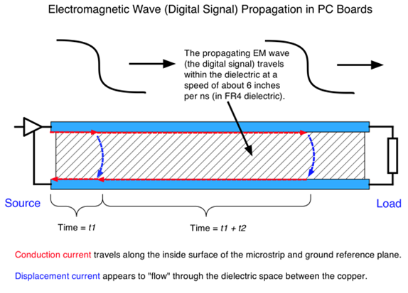 Figure 1. Digital signal energy is really an electromagnetic wave propagating through the dielectric space between the copper trace and return plane. The copper trace really serves as a waveguide.
Digital signals, power transients and RF propagates via an EM field within the dielectric space between the circuit trace and next closest metal (see Figure 1). We hope this next closest metal is actually an adjacent solid return plane! This EM field travels near light speed (about one-half light speed in FR4 dielectric) and induces electron flow, but at a speed of "drift velocity" or approximately 23 µm/s, which is quite slow.1 This is the current you would measure with an ammeter.
Knowing this, we must place a solid return plane adjacent to every signal and power layer in order to capture the EM wave and the entire path must not be interrupted by gaps in the return plane or when transiting from the top to bottom layers and vice versa.
At frequencies above 100 kHz, the EM field and associated conduction currents stay primarily under the circuit trace. In other words, the circuit trace can be pictured as a "waveguide." Because EM fields are largely trapped under the circuit trace, we can place other traces relatively close (three to five times the height of the trace above the plane, typically) and avoid signal coupling (crosstalk).
Where we can get in trouble is if a noisy clock signal and signals to/from a wireless module (or on-board antenna) share the same dielectric space. This causes noise coupling to sensitive receivers and associated poor receive sensitivity. One way to avoid this is through system and circuit partitioning, or, in other words, separating the noisy stuff from the quiet stuff.
Here are the rules for a quiet PC board:
- All signal layers must have an adjacent solid return plane
- All power layers must have an adjacent solid return plane
- When transitioning from top to bottom layers with critical (noisy) signals, use either stitching vias or stitching capacitors right at the signal via.
These rules dictate the board stack-up! The typical four- or six-layer board stack-up is a poor choice for today's high-speed RF and wireless designs; especially with the smaller boards used for portable and body-worn devices. This is not to say that these typical stack-ups won't work for simpler lower-frequency circuits, but I deem them high-risk for crowded mixed-signal or wireless designs.2
Let's look at the typical six-layer board stack-up I see often (see Figure 2).
 Figure 2. The typical six-layer stack-up has many EMC issues.
The typical six-layer stack-up has power and return planes too far apart for good high-frequency decoupling. In addition, any power rail transients will couple to layers 3 and 4. Finally, the bottom signal layer is referenced to the power plane. This is not necessarily a bad thing if the power and return planes are adjacent and closely spaced, but this is not the case here.
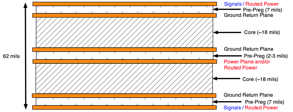 Figure 3. One of many possible improved six-layer stack-ups.
There are many other improved choices for a six-layer stack-up that follows low-EMI rules. Figure 3 shows one example where the power and power return planes are located closely for best high-frequency decoupling. In addition, all the signal and routed power layers have an adjacent and solid return plane. All return planes should be connected together with a 5 mm grid of stitching vias.
Quieting DC-DC Converters
Besides poor stack-up and layout design, I find that on-board DC-DC converters are one of the noisiest sources of self-generated EMI on wireless designs today (see Figure 4). Most of these are designed to switch at between 1 and 3 MHz, but use risetimes in the ns and sub-ns range.
The switch node pad and switch inductor can create a strong dV/dt (changing voltage with time), which creates a strong radiating E-field. These fields can couple directly into on-board or nearby wireless antennas and create a strong broadband EMI up through 1 to 1.5 GHz that can couple onto wireless receiver, GPS, and cellular modules.3
 Figure 4. Three DC-DC converter circuits are shown here. They can be easily identified by the large switch inductors.
There are several areas I look at when performing a design review of a DC-DC converter circuit.
- Is the converter specified one designed specifically for "low EMI"?
- Is the circuitry laid out completely on the top or bottom side of the board?
- Is there a solid return layer adjacent?4
- Is the input and output circuitry isolated from each other; that is, laid out as you would see on the schematic?
- Are there "sneak paths" coupling the noisy side to the quiet side? (This is part of the previous point.)
- Is the converter circuitry physically close to wireless modules?
- Is the switch inductor shielded and pin 1 connected to the switch node?
- Note that suggested layouts from data sheets are often incorrect from an EMC viewpoint.
TI, Analog Devices, and others are now developing "low-EMI" converters. TI has their "Hotrod" QFN package and Analog Devices has their "Silent Switcher" and "Silent Switcher 2" designs. The best of these include the input and output capacitors inside the package. Even better, some packages also include the switching inductor. This helps keep the switching loop currents minimized. These are more expensive, but worth it for very dense designs.
I had a client with a body-worn device locate most of the converter circuitry on the top side of their board, but located the switch inductor on the bottom side. The resulting 3 MHz switching currents (and associated EM fields) created a broadband EMI up through 1.5 GHz, coupling throughout the board and affecting the ability of the GPS module to hear the satellites.
Most buck or boost converter circuits will use an external switch inductor. Make sure to specify a shielded inductor to limit the radiating fields. Also, one trick is to ensure that pin 1 (the start of the winding) is connected to the switch node. The additional windings will act to self-shield the start of the winding, which will be switching at the input voltage (buck) or boosted voltage (boost). This alone can reduce emissions by 2-3 dB. Pin 1 is usually depicted by a dot, bar, or half-moon symbol.
Several manufacturers data sheets show a suggested layout with the input and output capacitors sharing the same return path. This will introduce switching transients on the power rail and couple this EMI throughout the board. I have also seen very large-area switch nodes. Because the switch node can create high dV/dt, the area of the pad should be minimized. Finally, some layouts do not indicate a solid return plane. Beware!
Mitigation Experiments
When you're not sure which DC-DC converter (or converters) might be affecting your wireless receiver sensitivity, there are a couple mitigation experiments you can perform. The first is to replace each converter with batteries.
This is actually very easy to accomplish. Simply remove the switch inductor. This will stop the converter and you now have easy access to the power rail. As shown in Figure 5, we simply wire in batteries across the inductor switch node to digital return. The use of regular power rectifiers can be added to drop voltages that are too high from the battery packs.
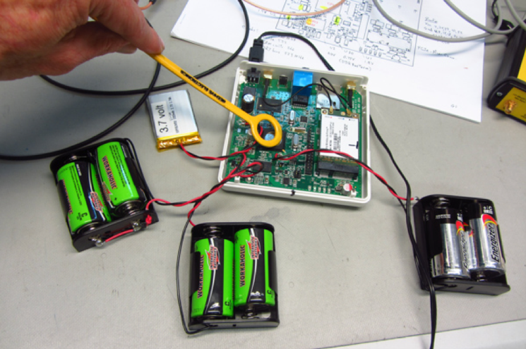 Figure 5. A demonstration of how to disable the DC-DC converters and replace with battery packs. Any voltages that are too high can be reduced with series rectifiers.
The second method would be to replace the converters with three-terminal linear regulators (see Figure 6). This is also accomplished by replacing the switch inductor and wiring the regulator between Vin, switch node and digital return. You may have to use adjustable regulators and an output voltage resistor network to set the correct voltage.
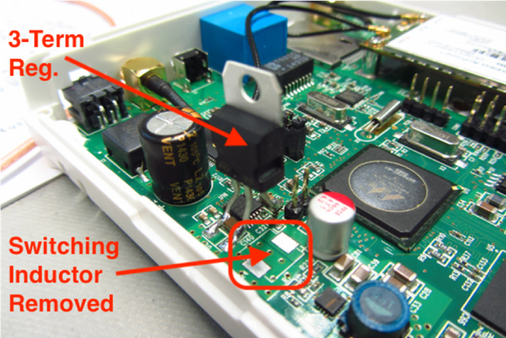 Figure 6. A demonstration of how to disable the DC-DC converter and replace it with a three-terminal linear regulator.
Field Reduction Techniques
This is a twofold design consideration: use of local shielding and application of flexible ferrite-loaded absorber.
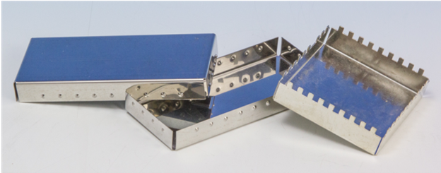 Figure 7. Several examples of local board shields are shown. They should be bonded in several places to the digital return plane.
Local board shields are most effective for E-fields and so are recommended to be placed over DC-DC converter or processor/memory circuitry (see Figure 7). They are partly effective for H-fields and therefore are sometimes placed over digital processing and memory circuits. When first laying out your board designs it makes sense to incorporate spots on the board where local shields may be bonded directly to the nearest return plane (see Figure 8). Without these bonding pads, it is difficult to add temporary shields after the fact. 5
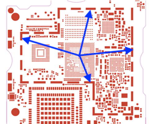 Figure 8. An example board layout that indicates places where a local shield could be bonded to the digital return plane. These bonding pads should be defined in advance in case a local shield is required.
 Ferrite-Loaded Absorber
One new mitigation technique I have been trying lately is the use of ferrite-loaded RF absorber.6 These come in flexible sheets of varying thicknesses with adhesive on one side. In my past designs of microwave modules, these could be stuck to the inside of shield covers to reduce structural resonances due to cavities.
Today, I'm using them to reduce the EM field level of IC packages and flex cables. The material is made by several manufacturers, such as 3M, Parker-Chomerics, NEC, and Würth Elektronik. They are either designed as near field communication shields or microwave absorber. For example, NEC has their R4N(01) material that has good absorbance in the cellular through GPS frequencies (blue trace as seen in Figure 9).
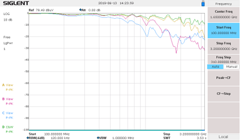 Figure 9. This plot shows the measured ferrite absorbers from NEC. NEC P/N EFR(01) is shown in yellow, FK2(03) in violet, 3TG(04) in green, and R4N(01) in blue. The measured samples were all 8×8 cm.
I had a chance to use this type material on a body-worn device a few years ago. The product included cellular, Wi-Fi, Bluetooth, and GPS. It also included a video camera that produced a high amount of EMI on its connecting flex cable. During characterization measurements, I identified the DRAM, power management IC (PMIC) and video cable as the highest energy sources of interference.
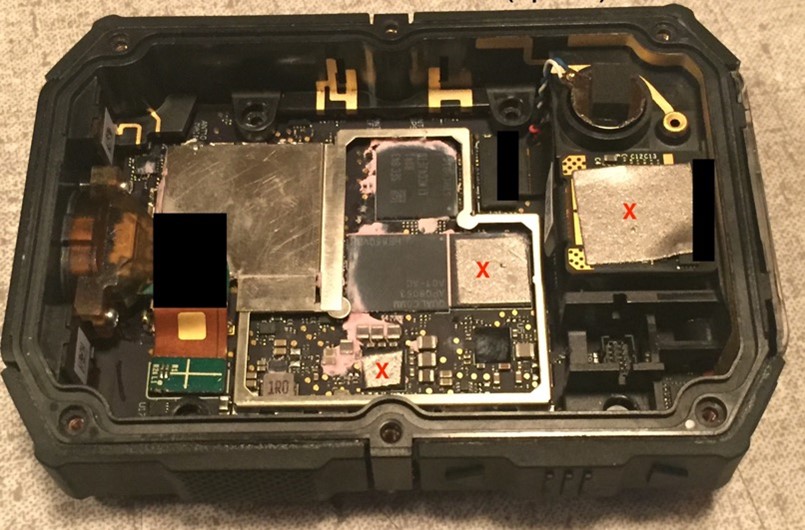
Figure 10. A wireless device showing three places where ferrite absorber was placed.
Placing small squares of absorber on top of the DRAM, PMIC and video cable (see Figure 10) were effective in reducing the self-generated EMI primarily affecting the various cellular receiver (downlink) bands.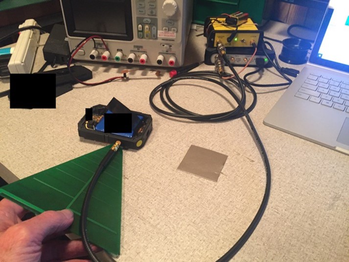 Figure 11. Characterizing the self-generated EMI using a close-spaced antenna.
In Figure 11, I'm measuring the near field emissions with a small antenna at the PC board edge close to where the cellular antenna is located embedded in the case. Examining the LTE Band 5 downlink band, we observe several signals that could be the cause of low receive sensitivity, including a large video harmonic (see Figure 12).
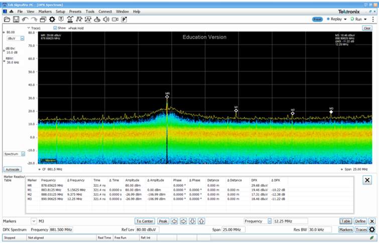 Figure 12. Looking at the LTE Band 5 downlink (869-894 MHz) which shows a strong video harmonic with several narrowband harmonics before the ferrite absorber was added.
Remeasuring the emissions, we see a 15 dB reduction in the video harmonic and the three narrowband signals have disappeared into the noise floor (see Figure 13).
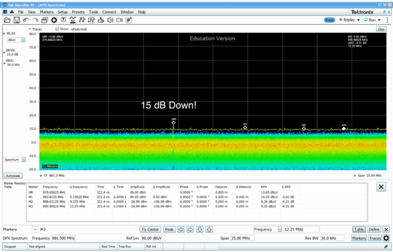 Figure 13. Looking at the LTE Band 5 downlink (869-894 MHz) with ferrite absorbers installed. The video signal was reduced by 15 dB. The narrowband harmonics were gone.
Video and LCD Displays
Video and LCD display circuits are special cases and typically use clock frequencies or data rates in the tens or hundreds of MHz. They typically require the use of flex-cables, which can act as radiating structures at wireless frequencies.
Often, manufacturers of these devices define the pinout poorly from an EMC point of view. That is, too few return wires, with several parallel video signals sharing the same return path back to the source. You will also find it necessary to bond the metal frame of any LCD display back to the digital return plane to keep the whole display from radiating as a "patch antenna".
Mitigations often include the use of flat ferrite chokes placed around these cables (see Figure 14), but I have been experimenting with the flexible ferrite absorber sheets, placing them over known radiating flex cables to absorb the EM fields. See previous example.
 Figure 14. A flat ferrite choke is often the solution to LCD display emissions.
One other mitigation is to design two-layer flex cables with one layer being a solid return plane to help capture and bound the field energy. It is important, though, to specify a connector such that at least one end of the plane layer is connected directly to the return plane in at least a couple spots. It would be better if both ends of the return plane could be bonded to the display or camera, but manufacturers of those devices never seem to make this easy.
Summary
In order to ensure the best receive performance for your wireless or IoT device, there are three key design aspects to consider:
- The PC board stack-up, routing and partitioning of noisy/quiet circuits is essential and usually the key factor in successful designs, especially those with mixed signal and dense layouts.
- DC-DC converters are a known strong source of broadband EMI and must be laid out correctly.
- Other high harmonic energy sources, such as processors, memory, LCD displays, and video cameras must have their fields reduced through shielding, ferrite chokes, or ferrite absorber sheets.
Many of these design issues can be addressed during the initial design stages or by characterizing the EMI on the bench top. Avoiding repeated trips back and forth to the compliance test lab will save time and money.
REFERENCES
- “Drift Velocity,” Wikipedia.
- K. Wyatt, “Design PCBs for EMI, Part 1: How Signals Move,” EDN, March 5, 2019.
- K. Wyatt, “Ten Tips to Minimize EMI from On-Board DC-DC Converters,” Interference Technology, May 16, 2019.
- S. Sandler, K. Wyatt, “DC-DC Converters – Solid Return Plane or Cutouts Under Switch Node and Inductor?” Signal Integrity Journal, July 28, 2022.
- K. Wyatt, “Local Shield Options for Wireless/RF Products,” Signal Integrity Journal, September 27, 2022.
- K. Wyatt, “Insertion-Loss Measurements of Ferrite Absorber Sheets,” EDN, July 25, 2019.