
When the converters’ inputs are sufficiently random, the quantization error’s distribution becomes uniform and becomes impossible to backtrack the exact input value. When this condition is true, quantization error can be treated as an independent noise source from other noise sources (ISI, thermal noise, etc.). It is also important to note that quantization noise’s uniform distribution makes it a bounded noise, which affects the system in drastically different ways compared to unbounded Gaussian noise. For the scope of this paper, SNR-based analysis will continue to be used as a proxy to compare system performance, but we recognize that such results do not translate to BER directly, though strongly correlated.
SNR-based System Analysis
When we model the converters simply as another noise source with its own distribution and noise power, we can apply the same SNR-based analysis as earlier in this study. For a uniform distribution bounded by  is the LSB size of the converter, the standard deviation (therefore RMS noise power) is
  By finding the appropriate
  for each architecture, we can incorporate the extra quantization noise into Equations (3) and (4).
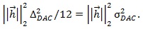
For the TX FFE architecture, the full-scale range of DAC (also known as  ) is the maximum swing allowed by the transmitter. Peak power constraint is already applied in the digital domain, thus the DAC’s full-scale range is
  =400mV, the same value used in the previous section. If the DAC has B bits, then its LSB size
  The
The  term is due to the fact that the DAC intrinsically has one fewer step than that of the ADC staircase. However, since we mainly deal with moderate to high resolution converters (e.g., >6 bits), the effect of this term is minimal. Therefore, we will treat the LSB size of DACs and ADCs to be the same with
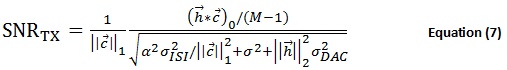
Since this quantization noise is on the TX side, it will be filtered by the channel, like the actual signal. Therefore, the received total noise due to quantization is multiplied by the L2 norm of the channel, given by:

Thus, the final receiver SNR for TX FFE is:
Now for the RX FFE architecture, the full-scale range of ADC is the maximum channel output. The theoretical maximum of the channel output is the maximum TX swing multiplied by the L1 norm of the channel. Thus, for an ADC with B bits, the LSB size  The ADC is followed by the FFE, which means its quantization noise is amplified by the L2 norm of FFE filter, like the RX input noise. The noise variance is then given by
 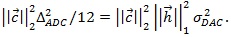 The final SNR for RX FFE system is:
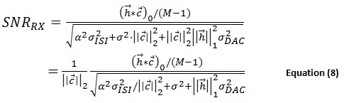
From Equations (7) and (8), we can see how the location of the quantizer affects system performance. The same conclusion still holds from the previous section if  is the dominant noise source. However, the SNR comparison becomes unclear when quantization becomes dominant. Even though the RX FFE has the benefit of
  overall, TX FFE architecture has the advantage of
  when it comes to quantization noise. Therefore, a more accurate comparison must consider the channel, quantization resolution, and other noise sources in the relevant system.
Simulation Results and Discussion
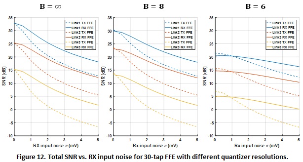
Similar to previous sections, we first plot system SNR against RX input noise using the analytical equations as shown in Figure 12. For this section, only the 30-tap setting is used. Results of infinite resolution converter is also shown as a reference. The overall trend and conclusion stays the same as previous analysis. As RX input noise becomes dominant, the RX FFE architecture still significantly outperforms TX FFE.
However, in a low-noise environment, TX FFE can provide better SNR, an effect due to channel filtering and more profound for low-resolution converters (B=6). On the other hand, system SNR degrades greatly when the resolution is too low, making the overall system performance unacceptable. Therefore, a more realistic quantizer resolution is typically equal to or greater than 7 bits. Under such settings, the quantizer effect almost becomes negligible and the same conclusions can be drawn as before.
Quantizers are also implemented in behavioral simulations to compare with the analytical results. Only the results for Link 2 are presented in Figure 13. Again, the SNR results from transient simulations match that of the theoretical analysis. It is interesting to note is that for low-resolution converters, the benefit of using adaptive RX FFE diminishes since the total system noise is dominated by quantization noise.
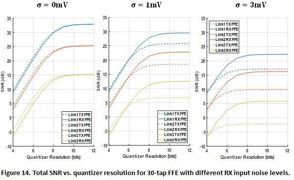
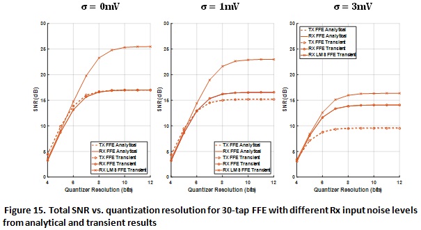
To visualize performance from a different perspective, SNRs are plotted against quantizer resolution at three different RX input noise settings as shown in Figure 14. For reasonable noise level (  ~ 1-3mV), system SNR plateaus at around 7 to 8 bits and RX FFE starts to outperform TX FFE. Transient results for Link 2 is also shown in Figure 15, and similar conclusions can be reiterated from the resulting plots.

To summarize, by adding converters in the system to utilize DSP either on TX and RX side, the overall system performance degrades due to quantization noise. Similar to the L1 vs. L2 norm effects when considering FFE coefficients, quantization noise also sees channel filtering and corresponding L1 and L2 norm amplification could be calculated given a channel of interest. TX FFE with DAC has more relaxed requirements in terms of converter resolution, but the RX input noise effect still dominates. To have reasonable system SNR and sufficient margin for variations, moderate resolution converters are needed and the advantages of TX side converters vanish.
Tradeoff between FFE length and Quantization
By studying Equations (7) and (8) again, one important observation can be made that there is diminishing margin of return by reducing ISI indefinitely when quantization noise is involved. As a result, the minimal benefit of having a more FFE taps might not justify the cost of implementation.
In this section, we explore the tradeoff between FFE length and quantization resolution using SNR as the metric, and show how RX and TX FFE differ in said tradeoff. Similarly, RX input noise will also play an important role affecting the final results. It is crucial to note that such analysis is channel dependent. Although only Link 2 is used as an example, the general trend and top-level conclusions would stay true while the absolute SNR values might differ.
Figure 16 shows the SNR vs. number of FFE taps for different quantizer resolutions under different noise environment. The black curves are used as references to show the infinite resolution quantizer results, which is identical to corresponding curves in previous sections. When  = 0mV, the TX and RX FFE provides the same system SNR for
  thus only one dashed curve is shown. We see that TX FFE can outperform RX FFE when no RX input noise is present, giving TX FFE an advantage. For this particular channel, in addition to steady performance increase until approximately 15 taps, there is another performance jump at about 25 taps. This means that the specific channel pulse response has large ISI components at about 16th post-cursor location (8 pre-cursors). However, this jump in performance is not as significant when quantizer only has 6 bits. This agrees with our intuition that there is no longer large improvement in SNR by increasing FFE length for lower resolution systems.
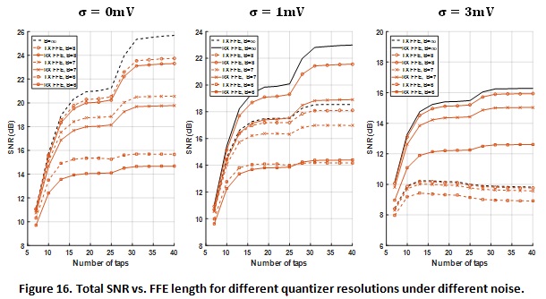
TX FFE’s advantage quickly disappears even with small RX input noise level. For  RX FFE at 7 bits actually provides better SNR performance than TX FFE at 8 bits. This has important implications due to implementation challenges for data converters at such speeds (Section 4). When large is present, TX FFE becomes completely infeasible, and having more taps in reality reduces SNR performance due to the peak power constraint.
Contour plots provide a better view of tradeoff between FFE length and quantizer resolution. As shown in Figure 17, when there is no RX input noise, TX and RX FFE provides similar performances. The best results happen with larger resolution and more taps. For high resolution quantizers (>8bits), there is still incentive to increase the number of taps, while for moderate to low resolution quantizers (<6bits), SNR almost follows the same color on the contour plot if number of taps is increased, indicating no significant performance gain.
Interestingly, for noisier RX input environment, TX FFE’s contour plot completely changes while RX FFE’s stay relatively the same. The overall performance decreases for both architectures, but the degradation is more profound for TX FFE. On the other hand, for TX FFE, increasing number of taps is no longer effective and in fact actually decreases performance. The peak performance actually happens at high resolution and just enough FFE taps. For RX FFE, performance peak is still at the upper right corner, but there is not much benefit to increase FFE length for 7 or 8 bits quantizer either.

Given a channel of interest and RX input noise level, we can find the optimal tradeoff between FFE length and quantizer resolution using contour plots similar to the examples shown above. In general, TX FFE can have better performance in a low noise setting, but RX FFE will be much better in other cases. Besides, RX FFE system performance tends to be monotonically increasing with respect to FFE length while TX FFE is further limited by the peak power constraint when maximum output signal is normalized to full-scale range.
Silicon Implementation Discussions
For high-speed links at and beyond 56G, system design becomes more intertwined with silicon implementation and realizability. Even though circuit design for such systems is a vast and important field in itself, we can still draw meaningful conclusions by studying top-level challenges and first-order comparisons. In this section, we discuss respective design challenges for DAC and ADCs, and use state-of-the-art publications to estimate circuit power to provide more realistic comparisons between TX and RX FFE architectures.
Challenges in high-speed DAC design
Despite many well-known DAC topologies, such as resistor string and R-2R DACs, current steering DACs are most widely used at high speeds. Currently, alternatives at such demanding bandwidth remain largely unexplored. One of the biggest challenges even for current-steering DACs is the large capacitance at the output node due to high current level and parallel connection of many unit elements, which can severely limit the TX bandwidth. Clocking tends to be the most significant challenge for such DACs, especially the distribution of the high-rate clock. High frequency SNR is often limited by jitter and static timing errors, which can typically only tolerate a couple of hundred fsrms. In addition, pre-drivers must typically be time interleaved (2x or 4x) and this leads to skew and ISI that must be mitigated.
As speed increases, there is no longer a clear line between digital and analog circuit designs. For such desired DACs, the digital data path design also becomes very challenging with many levels of clocking and parallelism. It is also not surprising to have this portion of the system to dominate power. For more advanced process technologies, wiring and layout parasitics have already become the more defining issues that restrict design performance. DACs tend to have long wires that require sophisticated extraction tools and many layout iterations.
Furthermore, finite S22 can lead to far-out ISI, which is a more pronounced issue for TX designs. Thus, sophisticated T-coil ESD structure must be designed together with the DAC, which adds another dimension to the already challenging task.
Challenges in high-speed ADC design
While ADCs face similar challenges compared to DACs at GHz sampling speeds, more research efforts have been put into building power efficient ADCs for various systems. Among all architectures, flash ADC is the fastest, but 7b resolution is impractical due to the large number of comparators needed. Current solutions rely on massively time interleaved SAR ADCs with quadrature sampling at the input and sub-ADC running at up to ~1.5 GS/s. Logic delay and metastability requirements make it difficult to make the sub-ADCs any faster. Technology scaling does not help much due to the dominance of wire parasitics.
Massive time interleaving requires lots of buffer power. This is also a strong function of ADC’s input capacitance and layout parasitics. As a result, the ADC’s input capacitance must be managed to maintain high bandwidth. At the chip input, desired bandwidth is achieved with carefully designed ESD structures, which typically comes at a cost of reliability.
ADC power tends to be evenly split among slices, interleaving network, and clocking. Generally, in this speed regime, power tends to grow proportional to the square of the clock frequency, making it very difficult to stay power efficient at high speed.
In order to take advantage of digital calibrations to reduce power, different methods for offset, skew and gain calibrations have been proposed and verified. It is much easier to have background calibration to ensure ADC robustness because the converter is on the RX side, just as the equalizer can be efficiently adapted. Furthermore, DSP equalizers can absorb some of the skew if separate banks are kept for each front-end sampler. These equalizer banks can optimally adapt their respective coefficients to boost performance, a feature that is difficult for TX FFEs to have.
Power consumption estimation between DAC and ADC
Even though a high-speed DAC’s performance is limited by its analog portions, clocking and digital tend to dominate power in modern designs. As a result, it becomes hard to estimate the power due to varying features and functions that might be included in the system. In addition, we must account for phase detectors, interpolators, etc. Furthermore, most high-speed DACs were previously realized in SiGe BiCMOS processes that are fast but high cost and not as scalable as CMOS processes.
By looking at some recent high-speed DAC designs in CMOS processes, we can estimate state-of-the-art power using technology node scaling. One of the most influential recent publications is [7], which is a 56GSps 6-bit DAC in 65nm CMOS. It reported a power of 750mW including test memory structure. For analog circuits, if a design is thermal noise limited, technology scaling does not really help due to kT / C constraint. For digital circuits, advanced technology processes begin to be limited not only by interconnect parasitics but also supply voltage scaling. Therefore, we assume a linear power scaling with respect to transistors’ gate lengths (as opposed to quadratic scaling). With [7] as the starting point, we estimate 210mW for a 6-bit DAC in 16nm, sampling at 64GSps.

The design reported in [8] is a full transmitter using an 18GSps 8-bit DAC. The reported total power is 144mW (84mW for transmitter and 60mW for clocking). If we only assume digital power for the system (which is optimistic in this exercise), we can estimate a total transmitter power in 16nm to be 300mW if it were running at 64GSps.
On the other hand, more research interest has been shown in ADCs during recent years and clear trends can be extrapolated from detailed surveys such as [6]. Figure 18 shows the energy efficiency of surveyed ADCs plotted against their signal to noise and distortion ratio (SNDR). Effective number of bits (ENOBs) of ADCs can be directly calculated from SNDR with Equation (9). The red circle on the plot highlights the region for recent published ADCs with approximately 6 to 7 ENOB. We see a power efficiency (energy per conversion) ranging from 1pJ to 10pJ.
A deeper investigation reveals that for high speed ADCs using interleaved SARs, the power efficiency is approaching 3mW/GSps (3 pJ). We estimate then for a 64GSps ADC (accounting for design margin for 112G application), the power should be around 192mW.
A different plot reveals similar estimates as shown in Figure 19. A typical figure of merit (FOM) used for high-speed ADCs (that are not fully limited by noise) is energy efficiency per conversion step, shown in Equation (10).

When this FOM is plotted against sampling frequency, we observe their linear relationship on a log-log scale, which indicates the extraordinary cost whenever we aim to double of speed of conversion. The red circle highlights what the frequency region 56G – 112G application requires, and we observe a FOM between 50-500 fJ/conv-step. Using an optimistic value of 50fJ at the frontier of current technologies, and assuming an ENOB of 6, we arrive at an estimate of about 205mW for a sampling rate of 64GSps.
Power estimates for both DACs and ADCs are quite similar at around 200mW to 300mW. However, we are more confident with the consistency of estimates for ADCs due to the vast amount of work and literature surveys. Technology scaling only provides a first order estimate for more advanced technology processes because of the nature analog circuits and layout parasitics. We have to acknowledge that DAC power estimates here are optimistic. Thus, it can be concluded that ADCs can be built to be more power efficiently.
Summary and Future Work
Converters have further elevated high-speed links’ bandwidth along with powerful DSP capabilities. Higher order modulations such as PAM4 are necessary for possible implementations of 112G links, and system architectures need to be compared carefully to build power efficient solutions. In this paper, we extensively discussed location of feedforward equalizers and their impact on system performance.
Treating our links of interest as discrete time filters and using sampled signal to noise ratio as a metric, we investigated the limitations of peak power constraint when FFE is on TX side, and noise boosting when it’s on RX side.
In the presence of RX input noise, RX FFE significantly outperforms TX FFE due to TX FFE’s output signal strength being reduced by the L1-norm of the FFE coefficients. Analytical expressions are derived for system SNR and behavioral simulations were run to show validity of the analysis. In addition to direct SNR performance advantage, RX FFE also allows adaptation that tracks environment and circuit variations when operating.
Converters are then included in the system model. Quantization is discussed and assumed to be an independent noise source in this paper. For moderate to high resolution DACs and ADCs, RX FFE still maintain its SNR advantages since the input noise effect is still more profound. Furthermore, there is clearly a diminishing margin of return for increasing number of FFE taps when converters are present. Contour plots can be used to find the optimal solution space and specify both FFE length and converter resolution. DAC and ADC power consumptions are estimated using recent publication data and extrapolated to next generation process technologies and speed.
For future work, decision feedback equalizers (DFE) can be incorporated into the system to study its effects with FFE together. The analysis needs to be extended into continuous time domain, and thus consider timing and FFE’s effects on jitter. There were also several recent publications on analog FFEs, such as [9]. The system impact of putting some FFE in front of ADCs also need to be fully studied, which requires in-depth research in circuit implementations as well.
Similar to most complex fields, it is extremely important to design link architectures and circuits together. It is no longer enough to simply evaluate link performances and specify components’ requirements without proper acknowledgement of the difficulties in silicon implementations. By understanding the nature and design challenges of crucial building blocks, we can gain meaningful insights into overall system performance and lead to innovative solutions.
This paper was originally presented at DesignCon 2018.