
Various coplanar waveguide (CPW) configurations have been investigated in the past. For example, CPW was proposed by Wen in 1969 [1], [2]. Gupta in [3] lists various types of CPW: CPW with finite dielectric thickness, CPW with finite width ground planes, CPW with a cover shield, conductor-backed CPW with a cover shield, conductor-backed CPW, multilayered CPW, asymmetric CPW and asymmetric CPW with finite dielectric thickness coplanar waveguide (CBCPW). Wolff examines CPW in [4]. Recently there has been a renewed interest in broadband characterization of transmission lines on both PCB and integrated circuits at millimeter-wave frequencies for 5G applications [5], for high-speed digital applications [6]–[9], and optical frequencies [10]. Specific transmission lines features have been investigated, from copper roughness modeling [11], [12], placement of vias in CPW [12]–[18], and comparison of CPW performance has been compared to microstrip in [19].
Stripline is the preferred transmission line in high-speed digital circuits. The benefit of stripline is that it supports TEM mode and therefore has no dispersion and no lower cutoff frequency. Striplines have low radiation, and in addition, far-end cross talk is zero as symmetry produces relative capacitive and inductive coupling to be approximately equal [20]. However, the width of the signal strip to height of the substrate must be fixed for a specific transmission line impedance, which limits the design flexibility of striplines.
An advantage of a CPW is in its design flexibility. CPWs can be made on thick substrates. The design criteria in a CPW to achieve specific characteristic impedance is the ratio of signal strip width and gap. (The ratio of the width of the signal strip and the height of the substrate does not need to be fixed to produce a 50-ohm line.) Characteristic impedance is independent of the thickness of the substrate as long as the gap size is smaller than the thickness of the substrate [1]. To avoid parasitic microstrip mode, the width of the strip and the gap has to be smaller than the distance to lower or upper ground. To avoid stripline mode, the gap has to be smaller than the signal line width.
Via-holes can be introduced in both striplines and CPW to prevent parallel-plate waveguide modes, but this in-creases fabrication complexity and cost. Further, airbridges can be introduced to remove the slotline (aka odd CPW) mode. CPW can be made smaller in size than compared to microstrip [21] and, therefore, striplines as well. In order to minimize parallel-plate modes, the size of the ground planes on the same layer as the signal line can be made smaller, making the structure finite ground coplanar waveguide (FGC).
In practice, the bottom of a substrate is usually metalized for structural support and to improve isolation between layers in a multi-layered board. The top metal cover is present as well in a packaged circuit, making most CPW structures conductor-backed CPW with a cover shield. This work investigates embedded conductor-backed CPW with a cover shield and finite-size grounds FGC applicable to multi-layered boards, such as Intel Architecture Platforms [22]. In this paper, comparison of stripline and conductor-backed FGC with a cover shield losses, modal analysis, and coupling are investigated.
Simulation Setup
Single line simulations are first performed for FGC and stripline using modal analysis in HFSS. For a single line, four modes were set for CPW and for stripline for a 4mil length of the lines. The results were then de-embedded to 1 inch using HFSS de-embed function.
Typical values for an FR-4 board were used in the simulations: r = 4:4, tan = 0:02 = 5:7 108. Groiss model [23] option in HFSS was used with roughness set to RMS=6 m. The same roughness was set to all metal surfaces. It is likely that the CPW performance in this case is underestimated because the roughness on the side of the signal strip, where the fields are concentrated, is lower [19]. All metals have finite thickness of 1/2oz, or t = 0:7 mils. Dielectric loss was modeled using the simple loss model.
Stripline dimensions were designed using Linecalc in Keysight’s Advanced Design System [24]. Dimensions of the substrate were initially used from a typical Intel-based multilayer board. In a multi-layer stackup, the layers are core, prepreg, and copper foil. In this simulation, the dielectric material is typical FR4 homogeneous substrate, and that core and prepreq have the same dielectric properties. Stripline signal width was set to w=7 mils, and the distance to either ground was kept at 9 mils to maintain 50-ohm impedance.
Conductor backed CPW with shield impedance was calculated in Matlab [25] using equations in [26] and ADS. Width of signal line was set to 7mils and the distance to ground was increased until the parasitic microstrip mode was minimized at the height of the substrate of h=12mils. The distance from the CPW to the ground plane was then set to 16mils. The gap is g = 4 mils for a 50-ohm-Ohm line. Transmission line impedance simulation in HFSS was then inspected by looking at the generalized S-parameters to see that the line impedance was implemented successfully.
Characterization of Losses
Simulated CPW and stripline modes are shown in Figures 1 and 2. Attenuation and phase constants have been simulated for all modes in HFSS. Dominant modes in CPW and stripline have large real phase constants 400radm and attenuation constants of ( 10 Np/m at 10 GHz). Other non-dominant modes in the simulation are evanescent.
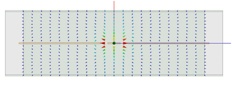
Figure 1. Vector representation of even (cpw) mode.

Figure 2. Vector representation of parasitic slotline (odd) mode.
To estimate the effect of each type of loss on embedded CPW, conductivity of copper, dielectric loss and roughness was sequentially added as shown in Figure 3 and 4. The worst-case scenario was used here, where all signal and ground surfaces are assumed to have roughness of 6 m. Graphs show that the roughness becomes important when the skin-depth is of the order of roughness (0.1 GHz). To make a fair comparison of losses in the bandwidth of interest, insertion loss and return loss are subtracted from the total power, as shown in Equation 1. Dielectric loss is the largest contributor to the overall loss.


Figure 3. Contribution of losses to CPW loss. (a) ohmic losses (b) ohmic and dielectric losses (c) omic, dielectric and roughness.
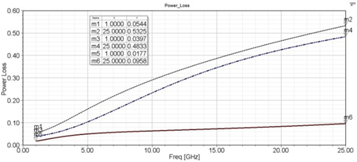
Figure 4. Contribution of losses to CPW loss. (a) ohmic losses (b) ohmic and dielectric losses (c) omic, dielectric and roughness.
Edge coupled CPW and Stripline comparison
In this section, two edge-coupled CPWs and striplines were simulated as shown in Figure 5. The horizontal separation gap between two striplines was varied from 5mils to 15mils in 5 mil increments. In CPW, the width of the center ground, between two CPWs was varied for the same distance. 4-mils thick line segments were simulated using terminal simulation, with one 996mils de-embedeed port. Waveports are assigned to the front and back side of the circuit, as shown in Figure 5. The size of waveport was selected so that the higher-order modes, including waveguide modes from the waveport do not propagate. Top, bottom and side grounds were selected as reference conductors, and three terminals were placed at left and right center conductor and the middle ground. Side grounds are designated as grounds through the edges of waveport. Middle ground terminals were renormalized to 10 6 to designate another ground conductor, and the center conductors were re-normalized to 50-ohm. Both CPW and uncoupled striplines are 50-ohm with return loss above 30dB.
In all configurations, CPW significantly outperforms stripline as shown in Figures 6 and 7. Dotted lines in Figures 6 and 7 show isolation and coupling for edge-coupled coductors separated by 5 mils, solid lines show separation of 10 mils, and dashed lines show separation of 15 mils. The top dotted line represents the stripline, and bottom lines CPW. The density of coplanar CPW lines can be significantly increased to produce the same coupling and isolation as in striplines. For example, coupling of two edge-coupled CPWs separated by 5mils is the same as two striplines separated by 15mils. The coupling in CPW can be further reduced by making the gap width smaller, therefore confining the fields tighter to the gap [27].
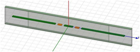
Figure 5. Edge coupled CPW lines.
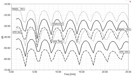
Figure 6. Coupling comparison for two edge-coupled CPW and striplines.
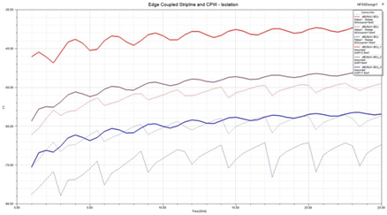
Figure 7. Isolation comparison for two edge-coupled CPW and striplines.
Broadside coupled CPW and Stripline comparison
Two broadside-coupled CPWs are shown in Figure 8, and the stripline was simulated in a similar configuration. Circuits were simulated using terminal simulation in HFSS. The distance between the broadside coupled lines was 4, 6 and 8mils. The labels on Figures 9 and 10 show the distance between the axis of symmetry, x-y plane, and each line. The simulation was performed in a similar way with the previous one, except this time, only the input port was de-embedded and renormalized to 50-ohm. The output waveport was not renormalized, which presents a perfect matched condition, and the S-parameters are normalized to a frequency-dependent impedance to present a clear difference between the isolation and coupling. The results would not be consistent with the measurements of a constant 50-ohm instrument, as in the previous simulation, but it is easier to see the difference between the coupling and isolation in two cases. Coupling and isolation in CPW lines is lower than the striplines. This is beneficial if the lines do not carry differential signals.

Figure 8. Broadside coupled CPW lines.

Figure 9. Coupling for two broadside-coupled Striplines and CPWs.

Figure 10. Isolation for two broadside-coupled Striplines and CPWs.
Conclusion
It is of interest in high-speed digital circuits to minimize the number of signal layers, limit layer transitions, and remove isolating ground layers in stripline to decrease layer count and, therefore, the price and weight of the multi-layer board. We show that the embedded CPW with a cover shield offers greater design flexibility and higher packaging density than stirpline for comparable coupling and isolation performance.
References
[1] C. P. Wen, “Coplanar waveguide, a surface strip transmission line suitable for nonreciprocal gyromagnetic device applications,” in 1969 G-MTT International Microwave Symposium, Conference Proceedings, pp. 110–115.
[2] ——, “Coplanar waveguide: A surface strip transmission line suitable for nonreciprocal gyromagnetic device applications,” IEEE Transactions on Microwave Theory and Techniques, vol. 17, no. 12, pp. 1087–1090, 1969.
[3] K. Gupta, Microstrip Lines and Slotlines, ser. ARTECH HOUSE ANTENNAS AND PROPAGATION LIBRARY. Artech House, 1996. [Online]. Available: https://books.google.com/books?id=gqeHQgAACAAJ
[4] I. Wolff, Coplanar microwave integrated circuits. John Wiley & Sons, 2006.
[5] J. Coonrod, “Managing circuit materials at mmwave frequencies,” Microwave Journal, vol. 58, no. 7, pp. 98–+, 2015.
[6] E. B. El-Sharawy, “Multilayer coplanar waveguide for high speed digital applications,” in 1992 IEEE MTT-S Microwave Symposium Digest, Conference Proceedings, pp. 979–982 vol.2.
[7] X. Guo, D. R. Jackson, M. Y. Koledintseva, S. Hinaga, J. L. Drewniak, and J. Chen, “An analysis of conductor surface roughness effects on signal propagation for stripline interconnects,” IEEE Transactions on Electromagnetic Compatibility, vol. 56, no. 3, pp. 707–714, 2014.
[8] G. Gronau and A. Felder, “Coplanar-waveguide test fixture for characterisation of high-speed digital circuits up to 40 gbit/s,” Electronics Letters, vol. 29, no. 22, pp. 1939–1941, 1993.
[9] Y. Qian, E. Yamashita, and K. Atsuki, “Modal dispersion control and distortion suppression of picosecond pulses in suspended coplanar waveguides,” IEEE Transactions on Microwave Theory and Techniques, vol. 40, no. 10, pp. 1903–1909, 1992.
[10] F. Fesharaki, T. Djerafi, M. Chaker, and K. Wu, “Low-loss and low-dispersion transmission line over dc-to-thz spectrum,” IEEE Transactions on Terahertz Science and Technology, vol. 6, no. 4, pp. 611–618, 2016.
[11] P. G. Huray, S. Hall, S. Pytel, F. Oluwafemi, R. Mellitz, D. Hua, and P. Ye, “Fundamentals of a 3-d snowball model for surface roughness power losses,” in Signal Propagation on Interconnects, 2007. SPI 2007. IEEE Workshop on. IEEE, Conference Proceedings, pp. 121–124.
[12] A. Sain and K. L. Melde, “Impact of ground via placement in grounded coplanar waveguide interconnects,” IEEE Transactions on Components, Packaging and Manufacturing Technology, vol. 6, no. 1, pp. 136–144, 2016.
[13] W. H. Haydl, “On the use of vias in conductor-backed coplanar circuits,” IEEE Transactions on Microwave Theory and Techniques, vol. 50, no. 6, pp. 1571–1577, 2002.
[14] Y. P. Lamy, K. Jinesh, F. Roozeboom, D. J. Gravesteijn, and W. F. Besling, “Rf characterization and analytical modelling of through silicon vias and coplanar waveguides for 3d integration,” IEEE Transactions on Advanced Packaging, vol. 33, no. 4, pp. 1072– 1079, 2010.
[15] G. E. Ponchak, C. Donghoon, and Y. Jong-Gwan, “Characterization of plated via hole fences for isolation between stripline circuits in ltcc packages,” in 1998 IEEE MTT-S International Microwave Symposium Digest (Cat. No.98CH36192), vol. 3, Conference Proceedings, pp. 1831–1834 vol.3.
[16] A. Sain, A study on the effects of ground via fences, embedded patterned layer, and metal surface roughness on conductor backed coplanar waveguide. The University of Arizona, 2015.
[17] A. Sain and K. L. Melde, “Characterizing the impact of conductor surface roughness on cb-cpw behavior via reduced computational complexity,” in 2012 IEEE 21st Conference on Electrical Performance of Electronic Packaging and Systems, Conference Proceedings, pp. 260–263.
[18] M. Yu, R. Vahldieck, and J. Huang, “Comparing coax launcher and wafer probe excitation for 10 mil conductor backed cpw with via holes and airbridges,” in Microwave Symposium Digest, 1993., IEEE MTT-S International. IEEE, Conference Proceedings, pp. 705–708.
[19] J. Coonrod and B. Rautio, “Comparing microstrip and cpw performance,” Microwave Journal, vol. 55, no. 7, pp. 74–86, 2012.
[20] E. Bogatin, Signal integrity: simplified. Prentice Hall Professional, 2004.
[21] T. Sporkmann, “The evolution of coplanar mmics over the past 30 years,” Microwave Journal, Euro-Global Edition, vol. 41, no. 7, pp. 96–96, 98, 102, 108, 111, 1998. [Online]. Available: ¡Go toISI¿://INSPEC:6049621
[22] K. Edwards and V. Ragavassamy, “Pcb stack-up overview for intel architecture platforms,” Layout and Signal Integrity Considerations, 2008.
[23] S. Groiss, “Numerical analysis of lossy cavity resonators,” Thesis, 1996.
[24] A. D. System, Release 2016. Santa Rosa, California: Keysight, Inc., 2016.
[25] MATLAB, version 9.2.0 (R2017a). Natick, Massachusetts: The MathWorks Inc., 2017.
[26] R. N. Simons, “Coplanar waveguide circuits, components, and systems. 2001.”
[27] G. Garcia and C. Chang, “Crosstalk between two coplanar waveguides,” NAVAL OCEAN SYSTEMS CENTER SAN DIEGO CA, Tech. Rep., 1989.
This paper was originally presented at EDI CON USA 2018.