
This paper is an Outstanding Paper Award finalist from EDI CON USA 2017.
As data rates for serial link interfaces, such as PCI Express® (PCIe®) Gen 4, move into the double digits, device modeling, interconnect modeling, and analysis methodologies must continue to evolve to address the shrinking design margins and increasingly challenging compliance criteria facing today’s engineers. To mitigate risk and optimize designs, it is critical to move analysis as far upstream as possible, to enable trade-offs, feasibility studies, component selection, and constraint capture.
Accurate modeling of SerDes transmitter and receiver equalization in the link are paramount to obtaining realistic simulation results, including the complex adaptive equalization that is present in nearly all high-data-rate serial links. Interconnect modeling also faces new challenges, with via arrays requiring full-wave 3D solutions in order to accurately characterize their complex via stub and coupling behavior, threatening to drive extraction times from minutes to hours or days. After simulation, interface-specific post-processing is often required to check transmitter, channel, and receiver compliance criteria.
This paper suggests methodologies for creating a “virtual prototype” of your serial link pre-design, and how to create the associated interconnect and SerDes models that go with it. We review how to utilize IBIS-AMI models, and how to build your own if they are not available when you need them. It also covers the latest interconnect extraction techniques to give you “full wave accuracy where you need it” while keeping computational times in control, and how to use standards-based compliance kits to automate post-layout analysis and signoff for advanced interfaces like PCI Express Gen 4.
As data rates continue to accelerate and supply voltages continue to shrink, the “unit interval” (UI) with which to interpret logic has compressed significantly (see Figure 1).

Figure 1 – Various PCI Express data rates running through 8” of FR4 stripline
With less margin to work with, it becomes increasingly important to move the signal integrity (SI) analysis process further upstream, to address issues and challenges earlier in the design process, allowing mitigation of risk at the back end of the process. This requires some shifts from traditional methodologies, as well as new techniques for modeling the serializer/deserializer, or “SerDes” devices that transmit and receive our high-speed signals. The fruit of this up-front labor is an optimized bill of materials (BOM) for the design, as well as constraints to enable a constraint-driven printed circuit board (PCB) physical layout process. Combined with efficient post-layout interconnect extraction and automated compliance checking, the goal is to be able to confidently sign off your design to fabrication, without major surprises or schedule impacts, and achieve success with your hardware, all while avoiding costly and time-consuming re-spins.
Moving Upstream with a “Top-Down” Methodology
One key element to a successful methodology for interfaces at these data rates is to move the starting point significantly upstream of the traditional post-layout verification step. There is a false notion that meaningful analysis cannot be performed until after detailed PCB layout is done, in a traditional “bottoms-up” methodology. Reality in a hardware design environment is actually quite different.
When the layout designer has completed a layout, there is typically a short time period of a day or two where engineers from the various disciplines (mechanical, thermal, signal integrity, power integrity, EMI) may get a chance to do a final review and provide some last minute inputs on the layout. But there will typically be considerable pressure from the project manager to release Gerbers to the PCB fabricator within a specified time slot, the assembly house will be lined up to order components and receive those bare boards for assembly and test, and the software engineers will be waiting for hardware to come into the lab so they can try out their latest software versions. In other words, a full Domino effect of supply chain dependencies will be captured in the project manager’s Gantt chart by the time PCB layout is initially completed, and the time available to perform detailed SI analysis at that point will be short. It is often more likely that you will “run analysis until you run out of time, then ship” as opposed to “run analysis until you are satisfied the interface will work, then ship.”
In order to accomplish a confident signoff for your critical interface in the compressed back-end of this PCB design process, preparation is critical. One strategy is to go “top down,” and build an early version of a simulation testbench of your serial link interface, well in advance of that late stage (see Figure 2). This can start upstream of detailed schematic capture, at the early BOM stage, when you get an initial understanding of the SerDes and protocol (ex. PCI Express Gen 4) that will be used to transmit and receive signals, a general idea of the partitioning of the system, how many PCBs will constitute the signal path, and what connectors will likely be used. Detailed models for all the blocks in the system are not critical at this early stage, and “placeholders” can be used initially, with the understanding that they will be replaced later as more detail becomes available. (Compliance kits are a rich source of preliminary models for your early testbench, and will be covered later in this paper.) In a nutshell, if you can draw the interface on a napkin, you should be able to put together an early simulation testbench. The benefits to this kind of top-down methodology are multiple:
- It makes you visualize the overall system, and the signal path that will be traversed.
- It helps you identify all the models you will need to complete the overall die-to- die signal path, so you can work on obtaining them before you need them.
- Getting something running early on makes you get your simulation testbenches set up ahead of time, so that subsequent runs throughout the process are largely a matter of updating models in the topology and re-running simulations in greater detail. This is a big time-saver at the back-end of the process, when time is short.
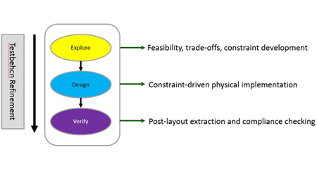
Figure 2 – General design methodology
With an initial prototype of your serial link topology in place, and at least placeholder models assigned to the various blocks, you should have a testbench that simulates and passes traffic at the targeted data rate. Now the work begins to replace models with more detailed, more realistic ones as you go through the design process. These models generally fall into one of these general categories:
- IBIS-AMI models for SerDes transmitters and receivers
- Spice models for discretes (ex. AC coupling caps)
- Packages
- PCB traces
- PCB vias
- Connectors
The first step is to do a gap analysis between the models you need for the various blocks in the topology, and the models you have on hand in your library. Augment your testbench with the models that you have, and verify that they simulate cleanly. Next, make list of the models that are missing, contact the model supplier (can be internal or external), and put in requests for the models that you need. Keep track of who you had contact with, the dates of contact, and the status of the model. As you get them, augment your testbench accordingly.
For the purposes of this paper, let’s assume that we are working on a PCI Express Gen 4 serial link, running at 16Gbps. Let’s also assume that we were able to obtain models for the AC coupling caps, packages, and connectors from your suppliers, as well as an IBIS-AMI model for your SerDes receiver. That leaves PCB traces and vias for the board to be eventually designed, and an IBIS-AMI model for your transmitter, which we will assume is currently unavailable from the supplier. Let’s first tackle the PCB structures.
Pre-Layout Modeling of PCB Interconnect
Modeling the PCB traces can begin by obtaining the proposed stack-up, including the material, dielectric and conductor thicknesses, impedance, line width, and spacing for the serial link’s differential pair. Next, identify which layer the main routing for the serial link (typically adjacent to a ground plane) will be, so that you can generate a microstrip or stripline model as applicable. With that information in hand, the next step is to estimate the length of the interconnect. For that a “floorplan,” or rough placement of the PCB is useful. Floorplanning tools will enable you to enter a basic PCB outline, a stackup, allow you to place parts from your footprint library, and even define some simple nets, all without a formal design, completed schematic, or netlist.
When looking at the floorplanning, don’t forget about the AC coupling caps. Will they be located on the top side of the board, where the SerDes devices typically reside, or will they be on the back side with most of the other discretes? This choice will result in different via configurations, so careful thought needs to be given at this point. Surface mount connectors also fall into this category, in the context of the overall system design.
From the floorplan, find the Manhattan length of the serial link as your starting point for PCB length (see Figure 3). Enter this information into your SI tool to generate a W-element model for the main PCB trace routing, and put this into your SI testbench.
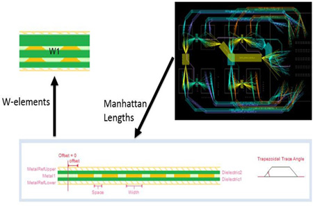
Figure 3 – Taking Manhattan lengths from floorplan for pre-layout trace modeling
Repeat this process for any other trace models needed for your testbench, including microstrip fanout traces, traces connected to either side of AC coupling caps, and so forth.
With nominal PCB trace models in place, attention can be turned to vias. Vias are a critical part of double-digit, multi-gigabit serial links. They generally represent the biggest “speed bump” in the overall signal path, and designing them such that insertion and return losses are minimized is crucial to successfully passing traffic at double-digit data rates. In some limited cases, it may be possible to eliminate vias with microstrip- only routing, but this is often not the case. The number of vias for high data rate serial links should certainly be minimized, but they typically cannot be eliminated.
Drill diameter, pad size, antipad design, and proximity to ground vias are all critical items. A key consideration for vias is the stub length, or unused portion of the signal path through the via, which can lead to reflections in the channel. Via stub length can be controlled by careful selection of routing layer, utilization of blind vias, or backdrilling (see Figure 4).
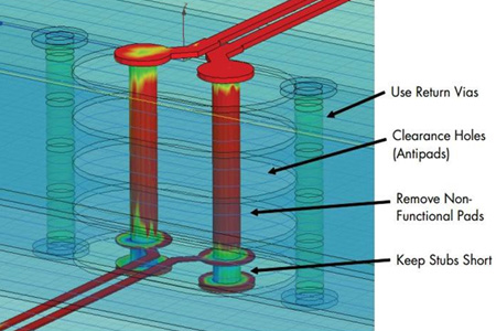
Figure 4 – Optimizing via structure parameters
Automated sweeping of these critical parameters can significantly accelerate the optimum via design for the serial link. Once the desired via structure is identified, it needs to be captured so that it can be implemented in the PCB layout. An automated mechanism for passing these via design parameters is very beneficial, as it ensures that they are implemented as intended in the physical layout, will be “correct by design,” and impact of the vias on final eye diagrams will be minimized.
IBIS-AMI Modeling
With initial PCB trace and via models in place for our hypothetical PCI Express Gen 4 serial link, the remaining missing piece is for an IBIS-AMI model of the transmitter, with “AMI” standing for Algorithmic Model Interface. As the name implies, an IBIS-AMI model has a “circuit” part, which is defined in traditional IBIS (I/O Buffer Information Specification) format, and an “algorithmic” part, defined in AMI format. Both are required for the complete model.
The circuit, or IBIS part of the model is used to describe the transmitter’s voltage swing, output impedance, parasitics, and rise/fall time characteristics. This information should be in the data sheet for your SerDes transmitter. Assume that the data sheet shows that the swing is around 1V differential into 50 ohm loads, with a single-ended 50 ohm output impedance, pad capacitance in the 0.5pF range, and single-ended rise/fall times around 20ps. This is fairly straightforward to put into a standard IBIS model as a starting point (see Figure 5).

Figure 5 – Preliminary IBIS model
The algorithmic, or AMI part of the model is used to describe the equalization behavior of the transmitter. In the case of PCI Express Gen 4, this consists of feed forward equalization (FFE), or “de-emphasis.” FFE will contain multiple “taps” that represent the main and boost drivers that produce the de-emphasis behavior, boosting transition bits (ex. 0 to 1 transition) and de-emphasizing steady state bits (ex. multiple 1’s in a row): see Figure 6.
The strength of these taps are usually described in terms of coefficients, that show their scale as compared to the main tap.
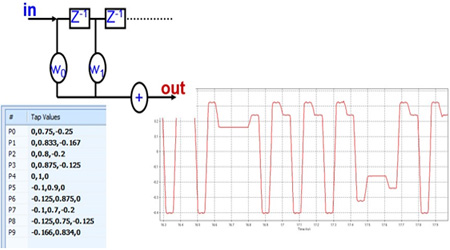
Figure 6 – FFE and transmitter waveforms, with PCI Express presets
IBIS-AMI simulation tools today often include utilities to generate AMI models directly, taking the information described above as input. Again, this information can typically be found in the data sheet for the SerDes transmitter. Assuming that the transmitter of interest uses similar de-emphasis settings to those described in the PCI Express specification, the tap coefficients shown above can quickly be used to directly generate an AMI model, using automated utilities as described earlier.
Enabling Constraint-Driven Design
With the pre-layout testbench built, populated with relevant models, and producing realistic simulation results, it is time to get constraints in place to drive and control the physical layout of the serial link. This may cause some refinement and iteration of the testbench in order to add additional detail, and this is expected. The approach at this point is to parameterize key elements of the testbench, sweep them to quantify their impact on the performance of the overall interface, and constrain those parameters to ensure that our design will meet the specification when finished. In the case of PCI Express Gen 4, the core requirement is for an eye height of at least 15mV and eye width of 0.3UI (which is about 19ps for a 16Gbps data rate), at the target bit error rate (BER) of 1e-12.
So what types of parameters are of interest to sweep? Let’s start with the SerDes devices. They will generally have circuit models with Fast and Slow corner parameters for silicon process/temperature/voltage (PVT), so that aspect should be covered. They may not necessarily be modified or controlled if you are the designer of the PCB, but their effects should be accounted for in sweep simulations, as your PCB will need to work under those conditions. Also, if you are able to obtain package models for the SerDes that cover the min/max range of interconnect parasitics, those should also be included. The same goes for connector and AC coupling cap models.
For the PCB interconnect, start at the transmitter footprint and work your way to that of the receiver. Today’s devices have fine pin pitches, and it is often necessary to neck down the line width and spacing of diff pairs in order to “break out” or “fan out” from the part. Those geometries will generally have a different (higher) impedance than out on the main part of the board, so that will impose an impedance discontinuity. How long can the fanout traces be before they cause a problem? This needs to be considered at the receiver end of the link as well.
Once out on the main portion of the board, the line width and spacing of the diff pair should be swept to replicate the impedance tolerances expected for the PCB (+/-10% is common). Also, it may be impractical to keep the differential traces together all the way across the board. They may need to spread away from each other and be briefly uncoupled to go around an obstacle, or even to connect up to the AC coupling caps. This will change the characteristic impedance. How long can they go uncoupled? How long can the pin escape traces for the cap be? Does that have a significant impact on the result?
And where do you locate the caps? Near the transmitter? The receiver? Does it matter? Sweeping the location can quantify the effect. What about the length tolerance between the positive and negative legs of the differential pair? Do the routed lengths need to be matched to +/- 1 mil in the layout? Or is it OK to allow 10 or 20 mils of difference?
Remember, it is just as important to figure out what does not matter as it is to figure out what does.
Crosstalk can have a major effect on serial link interfaces. If there is enough space on the board, it may be convenient to simply apply constraints for sufficient spacing around the diff pair to take crosstalk off the table as an issue. But many designs are too dense to accommodate that approach, which means that the spacing and coupled length of other signals to the differential serial link need to be considered and swept as well.
Overall length of the link is another basic factor. The equalization of the SerDes devices are designed to counteract lossy interconnect, but there are limits to what they can do. A very important parameter to determine is how long the overall routing can be, and still produce spec-compliant results.
These considerations do not comprise an exhaustive list of constraints to consider, but provide a good start:
- Fanout routing line width, spacing, length
- Main routing layer assignment
- Nominal differential line width and spacing
- Impedance tolerance
- Max uncoupled length
- Max via count
- Differential phase tolerance
- Max length from AC coupling cap to transmitter or receiver
- Max length of overall serial link routing
- Minimum spacing and max coupled length (parallelism) to other signals
- Via structure definitions
Incorporating these parameters into your pre-layout testbench enables them to be swept, and their impact quantified. The deliverable from this work is a realistic, implementable, and quantified set of constraints that can be imported into the physical layout process, and used by the layout designer to control the placement and routing of the critical serial link interface with automated design rule and electrical rule checks (DRC/ERC).
It is common for the layout designer to request some relaxation or modification of the initial routing rules. This is a natural part of the process, as sometimes some minor changes can enable a much cleaner and efficient design to be produced. And with the pre- layout testbenches in place, it should be straightforward to adjust some parameters, re-sweep, and assess whether the requested changes will significantly impact margins. This “negotiation” process may traverse several iterative loops, and will likely result in a better finished product (see Figure 7). The end goal from an SI perspective remains for the routed design to cleanly go through final verification and compliance checking, and produce acceptable margins.

Figure 7 – Incorporating constraints into layout to enable constraint-driven design
Efficient Interconnect Extraction
Once physical layout is complete (or at least the serial link differential pairs of interest are routed), post-layout verification can take place. One decision to make is to decide what bandwidth to use for the extraction. To assess this, it is necessary to consider the signals that will be passed through the link. The PCI Express Gen 4 spec refers to rise times of approximately 22ps, measured 10% to 90%. A classic expression relating the rise time to signal bandwidth is:
BW (GHz) = 350 / Trise (ps)
For the case of PCI Express Gen 4, we are looking at signal bandwidth of at least 16 GHz to start with, and likely higher as we factor in equalization. Most engineers would insist on a minimum bandwidth of several times the data rate, which puts us into the 30 to 50 GHz range. So for accuracy, we are clearly in the realm of full wave 3D electromagnetic field solvers, especially for complex, non-planar structures like coupled vias. So the initial inclination is to deploy full wave 3D extraction techniques for these types of serial links.
The problem is computational time. As discussed earlier, the point in the design process where you have detailed interconnect to extract is at the end. And the end of the design cycle is generally the most time-challenged of all, where you can least afford the long computational times. While 3D full wave methods are required for the complex via structures from an accuracy perspective, they are very slow for long, uniform transmission lines, like routed traces in PCBs. Fast, 2D methods still work quite well for those structures, so there is a basic conflict regarding extraction engines.
The most efficient techniques combine both methods, giving you “full wave where you need it”, while deploying faster, simpler methods to the long, uniform transmission line structures. This is generally referred to as a “cut and stitch” methodology, where the overall interconnect to be extracted is decomposed into different regions, depending on the specific interconnect structures found. Regions with 3D structures like vias are tagged for solution by full wave engines, whereas the regions with the long-uniform transmission lines are solved with 2D techniques.
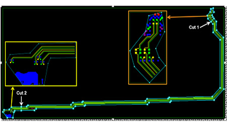
Figure 8 – Breaking interconnect into multiple regions for cut & stitch
The end results are combined together into one final S-parameter, as if the entire network was extracted with a full wave engine. The advantage of this technique is that it provides full wave accuracy, while providing solution times an order of magnitude (or more) faster than extracting the whole network with only a 3D full wave solver.
At this point, the detailed interconnect model(s) can be plugged back into your simulation testbench for post-layout verification, replacing the PCB trace and via models that were developed in the pre-layout stage.
Simulating with IBIS-AMI Models
By this point in the process, the SerDes component suppliers should have provided any missing IBIS-AMI models, which should be updated in your simulation testbench if they exist and are available. Now the focus shifts to post-layout verification. While it seems that we should be able to simply push the “simulate” button now with all the final models in place, there are often still things to consider with regards to IBIS-AMI models.
As discussed earlier, the algorithmic, or “AMI” section of the IBIS-AMI model represents the equalization functionality of the SerDes. At double-digit data rates, SerDes equalization techniques almost always employ real-time adaptation. To model this, AMI models will often have multiple settings available to the user, so that the equalization can be manually adjusted to best drive their specific channel. To figure out the best combination of settings, it is often left as “an exercise for the reader,” where the SI engineer has to sweep through the multiple combinations and figure out what works best.
With more advanced AMI models, the model itself will incorporate some or all of the adaptation into the channel simulation, closely emulating the behavior of the actual hardware. But even with these types of adaptive models, there are often settings to still review and optimize. For example, consider the following case, which uses a receiver AMI model that incorporates a continuous time linear equalizer (CTLE), automatic gain control (AGC, sometimes referred to as a variable gain amp, or VGA), and decision feedback equalization (DFE).
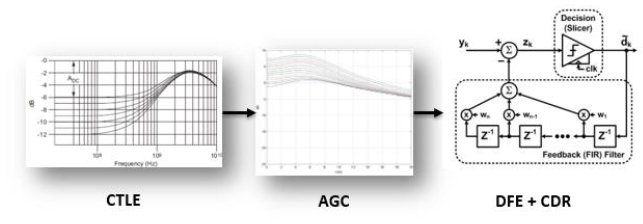
Figure 9 – Receiver equalization
In this particular model (see Figure 9), each sub-module (CTLE, AGC, and DFE) adapts their settings dynamically, so you may expect that no manual intervention is needed. Running with the default settings, the following is observed (see Figure 10).
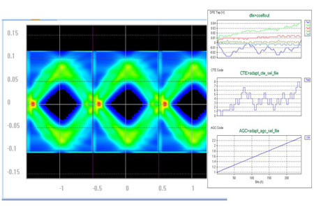
Figure 10 – Initial channel simulation results
While the eye has an opening, the plots of the CTLE, AGC, and DFE coefficients are showing that they do not really converge during the simulation, and continue to bounce around. The initial settings had the AGC module adapting twice as fast as the CTLE module. Speeding up the AGC adaptation to 4x, the CTLE adaptation speed yields these results.
With the quicker AGC adaptation, you can see that the coefficients for all three modules (CTLE, AGC, DFE) settle out and start to converge. But the convergence happens after about 150,000 bits of traffic are passed. So increasing the value of the “Ignore_Bits” parameter in the receiver’s AMI model from 40,000 to 150,000 will remove the first part of the simulation from the results, so the analysis tool evaluates the converged result, as would occur with the real hardware. This produces the result shown in Figure 11.
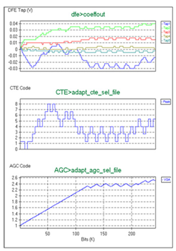
Figure 11 – Converged receiver equalization settings
Just by adjusting some of the interdependent AMI adaptation model parameters, the eye height in this particular case was improved from 40mV to 85mV at the target BER of 1e-12, an improvement of over 100% (see Figure 12).
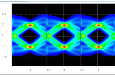
Figure 12 – Result with converged receiver equalization settings
This illustrates some of the subtleties associated with simulating with advanced AMI models. The user still needs to carefully review the documentation supplied by the model provider, understand the adjustable settings available to them, and leverage them accordingly.
Another capability related to equalization adaptation is backchannel training (see Figure 13). Many high-speed serial link protocols enable the SerDes receiver to evaluate the signal quality of training patterns sent by the transmitter, decide if it wants more or less equalization from the transmitter, communicate that request back to the transmitter, then receive another training pattern for evaluation. This process is repeated multiple times until the receiver is satisfied with the transmitter settings, then the actual data payload is transmitted with those preferred settings.

Figure 13 – Backchannel training
While the current IBIS standard does not support backchannel capability yet, there is a pending update to support this in IBIS with BIRD (Buffer Issue Resolution Document) 147, which will be incorporated into the next version of the IBIS specification.
Consider the PCI Express Gen 4 example (in Figure 14) with and without the utilization of backchannel training.

Figure 14 – Initial channel simulation results
The initial result (in red) is shown without backchannel enabled. In this case, the transmitter’s AMI model self-optimizes its FFE tap coefficients based on the characteristics of the channel, while the receiver’s AMI model adaptation is done real- time, throughout the channel simulation. The second result (in green) is with backchannel training enabled, and clearly produces a more open eye. The interesting item to note is that if you look at the difference between the FFE tap coefficients used in both cases, you will see that the FFE coefficients have been turned down in the backchannel case. For example, Figure 15 shows how the pre-cursor tap coefficient adapted during the back-channel training:
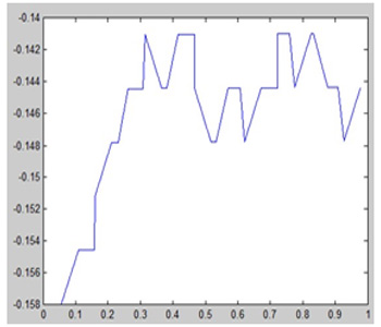
Figure 15 – FFE adaptation during backchannel training
Here you can see that the pre-cursor tap coefficient starts out initially at an absolute value of almost 0.16, and then over the backchannel training process, gets turned down to the 0.14 range, based on the receiver’s discretion. This enables the receiver’s more advanced equalization functionality to do more of the “heavy lifting” and ultimately produce a better overall result. This shows the importance of enabling the backchannel communication in the channel simulation process, and developing AMI models that closely emulate the real-world behavior of the SerDes devices in actual hardware.
Automated Compliance Checking
With detailed post-layout interconnect in place, and the IBIS-AMI models properly executing, attention can turn to compliance checking for the specific interface of interest, which is PCI Express Gen 4 in our example.
Each interface has some of its own specific criteria to be met. In this case, the PCI Express specification identifies a number of eye-related time domain criteria, frequency domain criteria for the passive interconnect channel, and also the ability to meet a specific jitter tolerance mask.
It can be very time-consuming to evaluate each of these criteria individually, especially if multiple runs are required to sweep corners and multiple channel models. Automated compliance kits for popular serial link standards are often available with simulation tools that can help dramatically speed up your compliance checking and accelerate your time to signoff (see Figure 16).
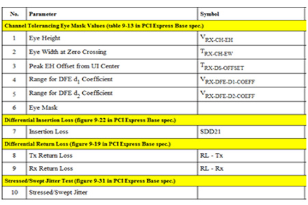
Figure 16 – PCI Express compliance checks
Automated sweeping of critical parameters and flagging of compliance failures (see Figure 17) enables better coverage of your serial link design, and helps to pinpoint any remaining areas of concern.
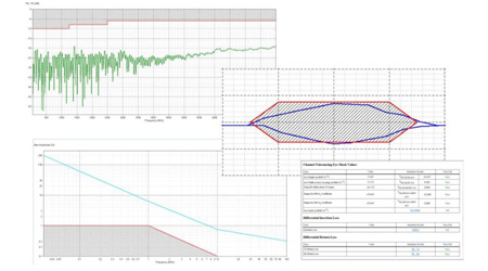
Figure 17 – PCI Express compliance results
The other major benefit to using compliance kits is the ability to leverage the associated templates in the pre-layout stage. As discussed earlier, it is critical to get an early testbench built for feasibility trade-offs. But it is common to lack realistic models for some of the necessary blocks at this stage, and sometimes “placeholder” models need to be used. The templates supplied with automated compliance kits will typically come pre-populated with realistic topologies and models, including spec-level models of the SerDes IBIS-AMI models for the transmitter and receiver, built to the reference parameters described in the specification for that particular standard. These templates, and the models associated with them, provide an excellent starting point for your pre-layout testbench development, help minimize the time needed to get up and running, and alleviate the need to start completely from scratch.
Summary
Serial link interfaces with double-digit multi-gigabit data rates have their own unique design challenges. A top-down analysis methodology, starting in the pre-design stage, is a valuable approach to mitigating the associated risks, and avoiding costly and time- consuming re-spins. The fruit of this labor is the wiring rules needed for constraint-driven physical layout. Special care needs to be taken with via structures to control insertion and return losses, and a method with which to enforce known good via structures into layout is essential. IBIS-AMI models are required to represent the adaptive equalization and backchannel functionality seen at these data rates, and can be quickly built to specification if needed. “Cut & stitch” approaches allow full wave accuracy to be deployed where needed for post-layout interconnect extraction, while avoiding the computational penalty of end-to-end full wave 3D extraction. Automated compliance kits can provide acceleration to confident serial link design signoff, while also providing valuable starting points for the pre-layout analysis stage.
Author(s) Biography
Ken Willis is a Product Engineering Architect focusing on SI solutions at Cadence Design Systems. He has nearly 30 years of experience in the modeling, analysis, design, and fabrication of high-speed digital circuits. Prior to Cadence, Ken held engineering, technical marketing, and management positions with the Tyco Printed Circuit Group, Compaq Computers, Sirocco Systems, Sycamore Networks, and Sigrity.
Acknowledgement
The author would like to thank Dr. Kumar Keshavan and Dr. Ambrish Varma of Cadence Design Systems, for the early IBIS backchannel functionality, and other contributions in the serial link analysis space far too numerous to mention.