The typically overstressed product manager is ultimately responsible for ensuring the final product works. Just engineering the power distribution network (PDN) can be a challenge when the three elements of the PDN have to be integrated together: the voltage regulator module (VRM), the interconnects and passive elements, and the power consuming elements. How can the product manager be confident, before the product is built, that all the PDN elements will play well together and meet the product performance specs, margin tests, and cost targets in all operating conditions?
One practical approach is to use some level of modeling for each element. This allows analysis of nominal and worst-case situations and, if necessary, exploration of alternative designs before final design decisions are made. An added benefit of this approach is that each design group can examine the models of the other elements and gain an understanding of how their element might interact with the rest of the system.
Selecting a model to use for each element in the PDN requires establishing a dynamic balance between acceptable simulation accuracy and the costs in effort, expertise, time, risk, and dollars required to attain that accuracy.
Although more detailed and accurate models of each element may increase the accuracy of the simulations, higher accuracy comes at some cost. Generally, the more accurate the model, the more complex it is, the more expertise is required to use it correctly, the more time it might take to run through scenarios, and the more difficult it might be to debug the results and build confidence in their accuracy.
If the model is so complex that only a few experts can understand it and use it without introducing artifacts, the risk of generating inaccurate results is high when less-experienced engineers use the model. On the other hand, if the model is so simple that it does not include features that might affect performance dramatically, it would have little value.
This paper reviews four levels of VRM models that VRM designers, board level interconnect designers, semiconductor designers, and product managers often use to explore design tradeoffs throughout the PDN system. The choice of which one to use involves considering engineers’ levels of expertise and what problems they expect to analyze. Some tradeoffs and relative merits of the models are described.
The Simplest VRM Model: An Ideal Voltage Source
The simplest VRM model is an ideal voltage source. This model has zero output resistance and is the worst model to use in any context because it does not predict any of the most important PDN noise behaviors.
Unfortunately, an ideal voltage source is used to represent the VRM in many time-domain power integrity (PI) simulations. The problem with the ideal voltage source is that it has zero impedance and shorts out (DC and AC) any PI component it is across.
We have attended many design reviews and found that this tendency of attaching an ideal voltage source as the VRM to the rest of the PDN is all too common. It is an unfortunate mistake made by many PI engineers. It is very important that ideal voltage sources are never used alone as the VRM model in PDN simulations, especially when impedance or transient responses to fast step current loads are being evaluated.
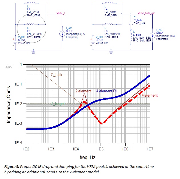
A First-Order Linear RL Model for a VRM
The simplest linear model that represents the VRM output impedance behavior, and is commonly used for frequency domain simulations, is a series RL model. This model has the advantage of being easy to implement and accounts for some of the interactions of the VRM with the rest of the PDN, from the die’s perspective, when simulating Vdd self-aggression noise. Of course, this simple model cannot begin to address the non-linear, stability, noise ripple, and saturation properties of a real VRM.
As illustrated in Figure 1, the output impedance rise of the VRM due to the internal feedback response bandwidth is well represented by an inductor and resistor. The resistor represents the VRM voltage drop that is proportional to DC current. The inductor provides an increasing impedance with frequency beyond some corner frequency.
The inductance value is calculated from the current ramp response time or by matching the resonant frequency between the VRM inductance and bulk (output) capacitance. Note that the inductance value for the simple linear model is not related to the inductor value in the SMPS model. The inductor of the linear RL model simply captures the behavior of the regulation loop (either SMPS or LDO), and does not represent any physical element. The resistance value (R) in the VRM model (R_VRM) is simply the resistance at DC or some very low frequency (100 Hz) at which the impedance curve bottoms out.
The R in the RL model needs to satisfy two properties: provide the correct damping for the parallel resonant peak and provide the correct DC output impedance. One single value can rarely do this. A more accurate model must include two values of resistance, and to be effective in the circuit, two series inductor values. This is a 4-element RL model.
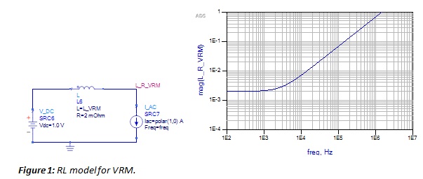
Second Order Model of the VRM: A 4-element RL Model
Modeling the VRM as the parallel combination of two series RL circuits, as shown in Figure 2, offers a simple, linear circuit model for a VRM that includes a more accurate representation of the DC or low frequency impedance, the equivalent inductance of the feedback loop, and the damping resistance needed to account for the first parallel resonant peak.
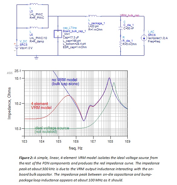
This 4-element RL model has little impact on the higher frequency Bandini Mountain peak but will affect the lower frequency parallel resonance between the VRM and the bulk capacitor. This model is useful when analyzing on-die Vdd self-aggression noise. The element parameters can be chosen to give reasonably accurate simulation results in both frequency and time domains with this linear model.
The second resistor (R_damp) is used to independently damp the impedance peak while the first resistor is used to set the proper DC IR drop. A good starting value for R_damp is the target impedance, which would result in a q-factor of 1. This can be refined by PDN measurement of an active VRM with a VNA.
The VRM will not deliver significant current at high frequency, so a second inductor with a value of approximately L_VRM/10 is used to model the blocked high frequency current. The 4-element VRM model provides the damping that brings the VRM impedance peak down to the target impedance without impacting the DC IR drop at low frequency. This is illustrated in Figure 3.