

Of the many webinars I viewed recently I came across these two very useful ones, and one quick-read paper.
Tim Wang-Lee from Keysight, presented a very nice tutorial on a design methodology for high speed serial links in this Keysight webinar, Robust Design Workflow for Signal Integrity. While this is a free webinar, you do have to register. Full disclosure, Tim is one of my PhD students and works full time at Keysight.
The old design approach is to make your best guess of the layout, build the board and test it. If it doesn’t meet the performance goals, you go back and redesign it, making some new guesses on how to improve the performance. This is a pretty inefficient process.
The new approach, Tim introduces, is to incorporate a pre-layout analysis step using rules of thumb and numerical simulations. He uses a USB channel as the example. He shows that to establish the design guidelines for this USB channel, it is remarkable how close to a final design he can get using just a handful of rules of thumb. “The power of rules of thumb gets you close to a final answer in a few seconds.”
By doing some up-front analysis with rules of thumb, which give you an idea of what you expect, you can then use the numerical simulation tool to develop a final virtual design. As Tim says, “anticipate before you simulate.”
With the initial interconnect design, the simulation tool can predict what happens to a USB, PRBS signal and what the eye might look like through this virtual channel. Figure 1 shows an example of the simulated eye, very close to his predictions using just a handful of rules of thumb.

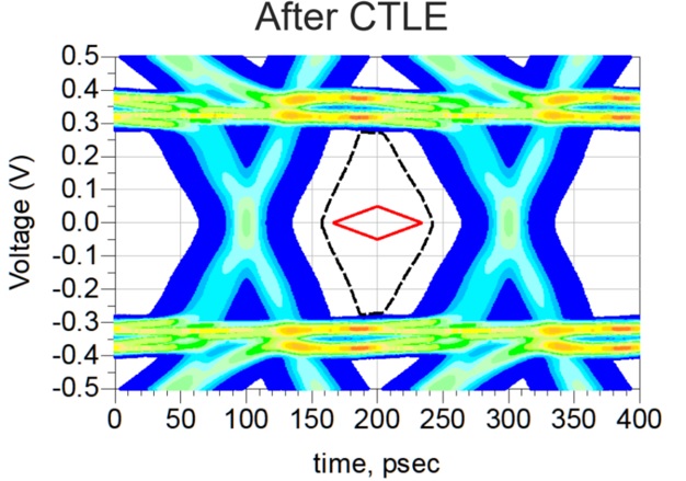
The final step before release to fab is a post layout simulation. In his example, he shows how an innocuous connection to an ESD protection diode in the USB signal path creates a 10 GHz stub resonance and its impact on the final simulation. In the virtual design environment, the final eye with the physical interconnects and random jitter with the RX CTLE included is predicted to be acceptable as shown in Figure 2.
With this new design flow, Tim says that you will have more confidence in the quality of your channels before you release to fab and a higher chance of first-time success. Check it out!
My second selection is the virtual Sensors Experience conference that Maxim Integrated put together. This is a glimpse into what future virtual conferences can be like. Figure 3 shows the welcome screen.

OK, so this is really a giant infomercial for the various products Maxim Integrated offers, but I still learned a lot. The experience is just like visiting a Maxim Integrated mega booth at a tradeshow. There are multiple kiosks, each demonstrating a specific product family, playing a 3-7 minute video.
I learned that an efficient buck-boost regulator could be used in a circuit to supply regulated power to a portable device from a supercap. The example used a supercap as a battery backup. While the supercap voltage is high enough, the regulator is in buck mode. When the voltage drops below the threshold, the regulator switches to boost mode to suck every last joule of energy from the super capacitor.
Like most tradeshow-conferences, there were also a few talks to attend, in the form of webinars. I watched one on the Critical Role of Actionable Insights for the Wearable Healthcare Revolution.
Traditionally, a wellness device is a consumer device you can buy off the shelf, without regulatory approval. A medical device is used in a clinical environment, regulated by some FDA like organization. The revolution is the greying of these areas: the merger of clinician recognized measurements in a consumer environment, like pulse oximetry, glucose monitoring and EKG measurements. This field is growing at a 20% CAGR.
And, my third “prince” for this column is a paper by Amit Bahl from Sierra Circuits, How to Choose PCB Materials and Laminates for Fabrication. There are a lot of papers and webinars posted by fab shops these days. This paper was the exception. I consider myself a bit of an expert when it comes to PCB technology, and I learned a lot from Amit’s Article.
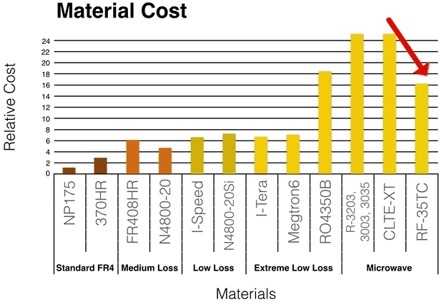
The starting place buckets to categorize laminates is by loss, from standard FR4 at one end to the RF/microwave ultra-low loss materials from Taconic, Arlon and Rogers at the extreme end. When loss is important in your application, the tradeoff is selecting the lowest loss materials you can afford. Figure 4 is an example of the relative cost for different low loss materials.
But loss and direct costs are not the only criterion. Amit offers a brief discussion about glass weave. He points out a denser glass yarn means more uniform glass, and more robust drilling. Check out his recent article and you may walk away with a few new insights as well.