
That moment of truth; pressing the power button and confirming that the power rail ripple does not exceed the design specification. If the designer waits until the delivery of hardware to integrate the power supply, the PCB power distribution network (PDN), and the dynamic switching load, it may be too late to avoid the headaches of intermittent data dependent failures. Understanding a few simple power integrity (PI) fundamentals can go a long way towards increasing design margins when delivering power to high-speed digital loads. If I had one word to describe power integrity, I would say “impedance”. This one word tells us that power delivery to high-speed digital loads is not a DC problem, it is AC. The simple impedance vs. frequency plot provides a wealth of design information on how to transition between the three sources of power for a high-speed digital load: the power supply, the PCB decoupling capacitors, and the package+die capacitance.
Lesson one in PI fundamentals is understanding how to read the impedance chart. The best way to do that is to look at simple models for these three sources of power. The power supply delivers power up to the bandwidth of its control loop and in its simplest form can be modeled as a low pass series R-L circuit. The PCB PDN power delivery is done by the total C of the decoupling capacitors, but capacitors are also limited in frequency by a series ESR and ESL term. The resulting simple model for the PCB PDN is a bandpass series R-L-C model. Finally, the packaged IC relies on the much smaller internal capacitance with very low ESL to deliver the GHz dynamic current to the switching transistors. A simple series C-R model captures this high pass behavior. Figure 1 shows the impedance plot of all three power delivery sources plotted separately and what happens when they are connected together. The impedance plot with the three sources of power connected together shows why the disconnected design approach can be so dangerous. If there is not a proper handshake of impedance matching when connecting these three power sources, then inductors and capacitors will resonate. These resonances are indicated by the high impedance peaks when connecting the three sources together in a simple AC simulation. If excited by the digital load, these resonances can create large swings in power rail ripple.
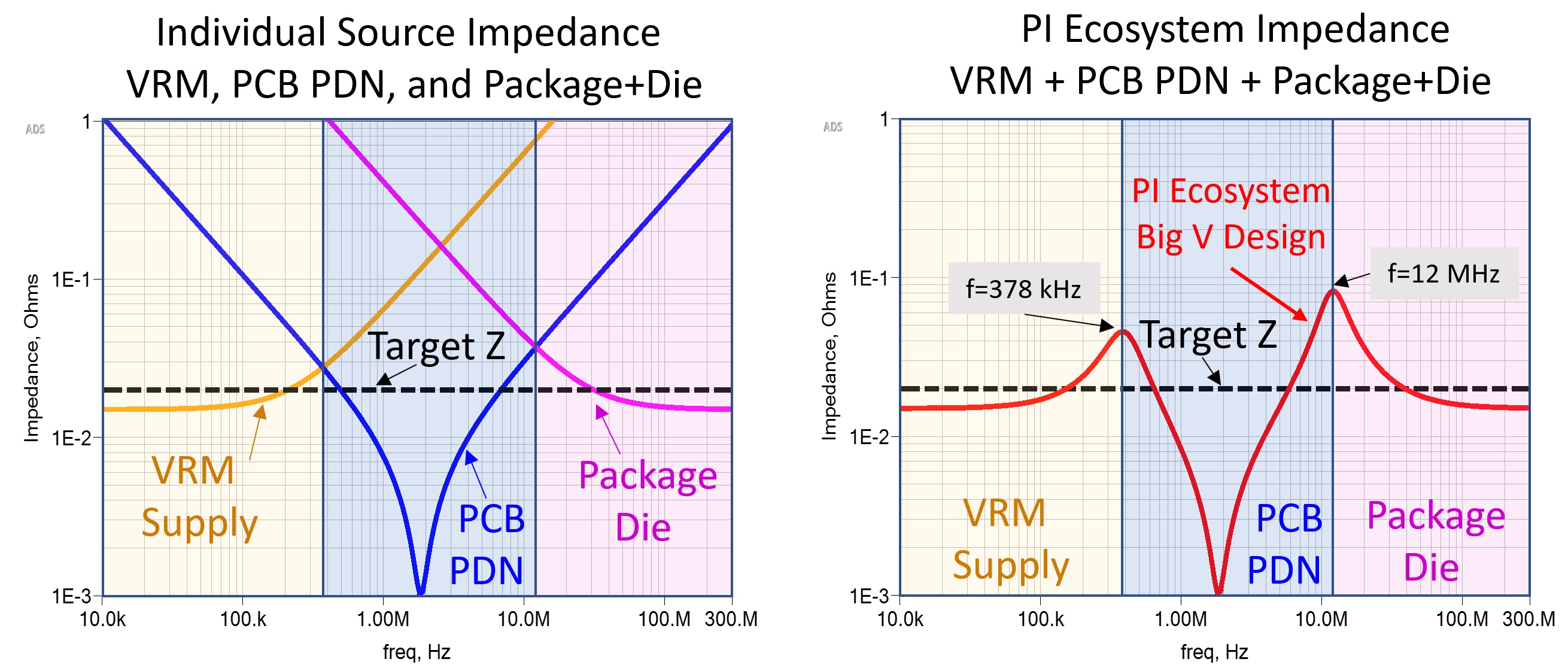
Figure 1: Power integrity uses the impedance domain to see how power transitions between the three sources of power: the VRM, the PCB PDN, and the Package+Die. The plot on the left shows the impedance of each power source separately. The plot on the right shows the danger of resonances for the Big V PCB PDN when the three sources of power are connected together.
The log-log plot of impedance vs. frequency in Figure 1 makes it easy to see what the problem is and how to engineer the power rail for resonant free matched power delivery or flat impedance vs. frequency. The trick to impedance plots is that the log-log scaling turns Capacitors into downward  slopes, inductors into upward
  slopes and resistors into flat lines. Parallel L-C resonances can result in
  resonances that show up as impedance peaks with a sharpness or Q that depends on real series resistance. The dynamic
 load current, times this impedance, can result in excessive power rail voltage ripple. To fight this problem of high impedance resonances in the power delivery, the PI engineer uses the concept of target impedance.
Target impedance comes from the simple estimation that power rail ripple delta V equals impedance Z, times the dynamic load current delta I. This is applied across the wide bandwidth of DC to GHz operation of modern-day digital loads [1]. Given a maximum ripple allowed by the load and a maximum step change in load current, then this will set a maximum target impedance to design to. All too often the maximum step change in load current is unknown, and designers use over simplified estimates, like 50% of the data sheet maximum current. Another option is to look at the series C-R model of the load and use this to provide matched power delivery free of resonances in the impedance domain. The IC vendor may not know the dynamic current, since this will depend on the application’s digital payload, but they can provide[IN1] [HB2] the impedance of the package+die power rail.
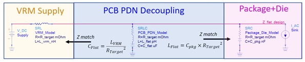
Figure 2: This simple schematic captures the PI ecosystem interaction of the three sources of power delivery to the GHz switching load. The PCB C must match to the VRM inductance, and the PCB L and R must match to the load to avoid high impedance peaks.
Designing for flat impedance, as shown in Figure 2, is not that hard for this simplified example of the PI fundamentals. First, the C-R model of the load is matched by the PCB PDN to find a maximum PCB  As the PCB PDN impedance increases inductively with frequency and struggles to deliver power, then the package+die smoothly takes over with its capacitance to maintain the resistive nature of delivering power. The resistive behavior keeps the impedance vs. frequency flat with voltages and currents in phase. This maximum PCB inductance L can be estimated as
  . Next at the lower frequencies, we need to transition to the power supply and the PCB PDN must have enough bulk charge storage to smoothly deliver power as the power supply inductance starts increasing the impedance to the supply. Again, this is a simple estimate of PCB
 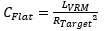 . These two simple estimates for the PCB PDN C and L quickly flatten the impedance vs. frequency and result in resonant free power delivery as shown in Figure 3. The PCB PDN with the Big V decoupling design has two resonances that when excited by the dynamic load, can add together and create a rogue voltage wave [2]. The Flat Z Design is considered to be critically damped with no over- or under-shoot ringing in the power rail voltage when the load current changes [3].
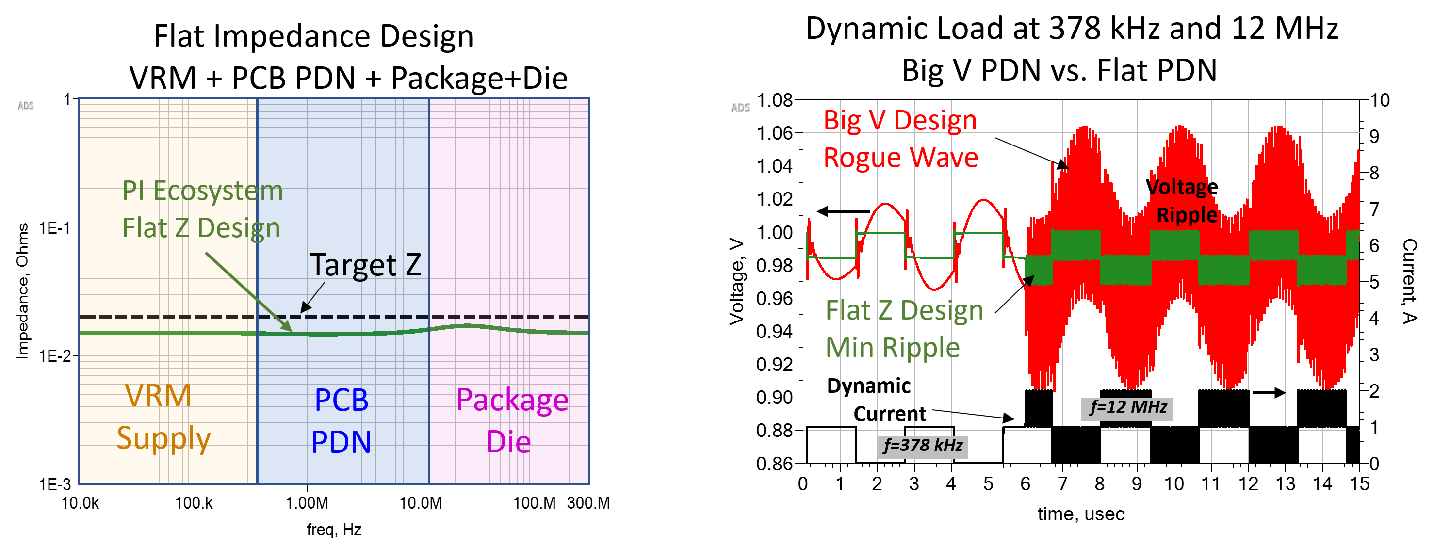
Figure 3: Flat impedance design with matched impedances in the frequency domain shown in the plot on the left results in resonant free power delivery in the time domain plot on the right. The plot on the right shows the dynamic current on the right axis and the resulting power rail voltage on the left axis. The Flat Z Design is critically damped with no over- or under-shoot while the Big V design has a rogue voltage wave when resonances at 378 kHz and 12 MHz are excited.
Flat impedance power delivery has additional benefits besides avoiding resonances. These benefits include minimizing the number of capacitors to meet a target Z, less sensitive to component tolerances, and avoiding unstable power supply oscillations. A quick look at 10% component tolerances with a Monte Carlo simulation, Figure 4, shows the Flat Z design will result in not just wider design margins, but less product to product variation when compared to a Big V design.
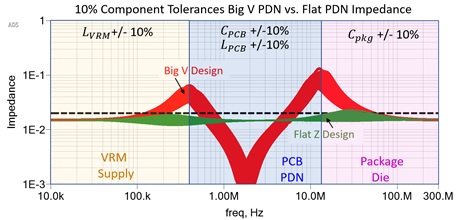
Figure 4: Monte Carlo simulation with 10% component tolerances to show that the PI Ecosystem Big V Design has more variation than the Flat Z design.
The simple flat impedance estimates are a great starting point for optimizing the power delivery with EM models of the PCB PDN to capture the power distribution parasitics. [4] In the same way that the three main sources of power are analyzed, one can also think of the PCB decoupling capacitors as an array of power sources, and like before, each capacitor’s ESL inductance has the potential to resonate with an adjacent capacitor’s C. One can sequentially add the capacitors starting at the supply with the largest bulk capacitors and work down to the smaller ones closer to the load using the simple equations for flat impedance. However, the balancing act required between the large quantity of decoupling capacitors can be very dependent on the PCB interconnects and parasitics. This makes decoupling capacitor optimization difficult to get correctly with simple estimates, and final optimization should be completed with a decoupling capacitor optimizer tool. A tool like Keysight’s PathWave ADS with PIPro in Figure 5 makes it possible to optimize the impedance of the full PI ecosystem by including models for both the VRM and the Package+Die.
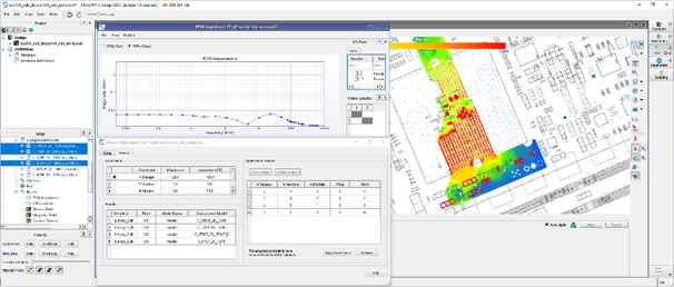
Figure 5: Optimizing the PI ecosystem in the impedance domain using the PathWave ADS PIPro EM tool to capture PCB position dependent parasitics of the decoupling capacitors. Optimization includes VRM, PCB PDN, and the Package+Die.
In summary, if you are working on high speed digital electronics, you need to know about the Power Integrity of getting power to the load. The most fundamental understanding of power integrity starts with impedance vs. frequency. This impedance vs. frequency information makes it easy to understand how the three sources of power: VRM supply, PCB decoupling, and packaged+die work together to deliver the power to the load. The optimum power delivery design has been shown to be a flat impedance vs. frequency design. Flat impedance results in the minimum number of capacitors to meet a required target impedance, reduced sensitivity to component tolerances, and matched impedance for resonant free power delivery that avoids rogue voltage waves. Remember to start early in the design cycle to leverage these Power Integrity fundamentals and make the best engineering trade-offs for your next high-speed digital design.
References
1. H. Barnes, J. Carrel, and S. Sandler, “A Method for Dynamic Load Current Testing with a Benchtop Power Supply”, DesignCon, 2020.
2. S. Sandler, “Target Impedance Limitations and Rogue Wave Assessments on PDN Performance” Signal Integrity Journal, March 19,2018.
3. I. Novak, “Comparison of Power Distribution Network Design Methods” DesignCon 2006.
4. S. Sandler, “How to Design for Power Integrity” Keysight sponsored YouTube Video Series: http://www.keysight.com/find/how-to-videos-for-pi.