
This paper is an Outstanding Paper Award winner from EDI CON USA 2017.
The current focus on power integrity is related to maintaining a low and flat impedance at high-speed devices such as memory devices, FPGAs, CPUs, and SerDes transceivers, as a few common examples. The singular goal is to ensure a stable supply voltage, within the specified range, to these high-speed devices as their load currents are dynamically changing.
Power integrity is a much broader topic that applies to low-power circuits as well. Many low-power circuits are hypersensitive to power supply noise. Examples of hypersensitive circuits include clock oscillators (XOs), low noise amplifiers (LNAs), phase locked loops (PLLs), mixers, and precision voltage references, to name just a few.
The most common performance metrics of these sensitive circuits include voltage and current noise, phase noise, timing jitter, and spurious signals. These characteristics are often affected by power supply noise, though the relationship between circuit performance and power supply noise is rarely defined.
This paper illustrates how the performance of these sensitive circuits can be degraded by power supply noise, how to quantify the sensitivity to power supply noise, and how to design a power supply for optimum performance.
Sensitivity to Power Supply Noise
When a noise signal is presented to a non-linear circuit, individual frequencies are multiplied, resulting in mixing products. For example, the simple circuit shown in Figure 1 contains a 100 MHz signal with DC offset to bias a silicon diode. A second, 500kHz signal is also applied to the diode. The diode is a nonlinear element in which the voltage is related to the log of the diode current.

Figure 1 Simple model of two sinewaves connected to a silicon junction (diode)
A harmonic balance simulation is performed to show the harmonic content of the diode voltage. With the 500kHz amplitude set to -65dBm, only the 100MHz signal is observed as seen in Figure 2.

Figure 2 100MHz and DC Bias with 500kHz set to -65dBm amplitude level
The amplitude of the 500kHz signal is increased to -30dBm in Figure 3. The 500kHz signal does appear as noise at 500kHz (not shown), but also appears as the sum and difference frequencies 100MHz + 500kHz and 100MHz − 500kHz. The 100MHz amplitude remains relatively unchanged.

Figure 3 100MHz and DC Bias with 500kHz set to -30dBm amplitude level
Further increasing the 500kHz signal to -10dBm shows that the non-linearity also adds the sum and differences of the 500kHz harmonics as seen in Figure 4.

Figure 4 100MHz and DC Bias with 500kHz set to -10dBm amplitude level
Most circuits are constructed from silicon junctions; therefore, they exhibit this nonlinear phenomenon. These sum and difference (or mixing) frequencies are a measure of the performance of oscillators, LNAs, ADCs, and other sensitive circuits. Although these mixing frequencies can be generated from multiple sources, one of the most common, and often dominant, sources are power supplies.
Defining Sensitivity
It is often difficult to determine how much power supply noise can be tolerated because the information is not generally published in the component datasheets. Also, there is a very large variation among manufacturers and even different models within a single manufacturer’s product line.
For example, in the case of a crystal oscillator there are many oscillator topologies; some incorporate internal PLLs, internal voltage regulators, or filter components. Although these internal circuitry details are generally not published, the effects can be seen in phase noise or jitter measurements.
Phase noise plots for two different 125 MHz clocks illustrate this difference in Figure 5. One plot shows a characteristic hump, generally the result of an internal PLL, while the other does not. The two clocks also have significantly different integrated time jitter, with one at 377 fs and the other at 1.5 ps.

Figure 5 Phase noise plots for two different 125MHz clocks from two different manufacturers
A line injector connected to a Gaussian noise generator is used to modulate the power supply while measuring the clock phase noise on a signal analyzer. The setup for one of the clocks, located on a Picotest VRTS3 demo board, is shown in Figure 6. The same setup is used for the second clock.

Figure 6 Picotest VRTS3 demo board with J2120A line injector measuring 125MHz clock spectrum
The same wideband noise voltage is added to each of the two clocks to see the impact on phase noise. The plots in Figure 7 compare the phase noise of the two clocks with and without the injected noise. The Silicon Labs 571 clock is insensitive to the power supply modulation noise because it includes a high noise rejection voltage regulator inside the clock. The phase noise of the other clock, a Fox Xpresso, is degraded nearly 25 dB due to the power supply and a low-noise power supply design will be required. The Xpresso clock also appears to have an internal resonance at 150kHz, which is evident along with all of the harmonics of this resonance. This noise sensitivity should be carefully weighed in the selection process. The extra cost and physical board area consumed by power supply components might be better spent on a low-sensitivity clock. Still, there are many sensitive circuits that will be sensitive to power supply noise, and this paper will show how to design low-noise power supplies.
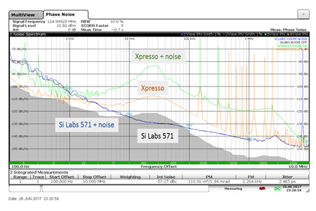
Figure 7 Phase noise plots of the two clocks with and without power supply noise added. Selecting a clock that is less sensitive to power supply noise is one way of reducing phase noise.
Defining Power Supply Noise Limits
The optimum clock performance is determined by measuring the phase noise using a near ideal power source. This establishes the optimum performance of the clock, which is shown in Figure 8 along with the noise from two higher noise power sources.
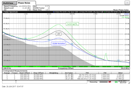
Figure 8 Clock phase noise powered by a J2120A line injector with zero modulation, essentially a “noiseless” power supply, as well as two other power supplies
The direct voltage noise density measurements for the three power sources used in Figure 8 are shown in Figure 9.

Figure 9 Voltage noise of the J2120A line injector, an LM1086 LDO linear regulator and an LMR10515 POL switching regulator
Next, the phase noise of the sensitive clock is measured using the three power sources shown in Figure 9. The results are shown in Figure 10.

Figure 10 The phase noise of the sensitive clock using the same three power supplies measured in Figure 9. Note the 2.9 MHz spur apparent when powered by the switching regulator.
Designing a Power Supply Noise Filter
Both the tolerable power supply noise and the required noise reduction can be determined from the “noiseless” source plot in Figure 8 and the increase in noise when powered by the voltage regulators in Figure 9. Most voltage regulator noise is due to the internal voltage reference and so cannot be removed at the input to the regulator, only from the output of the voltage regulator. Removing the power supply noise using a post-regulator filter requires attenuation equal to the phase noise degradation. For example, a filter would need to provide 6dB attenuation at 5kHz for the added noise from the linear regulator and a filter with 14dB attenuation at 5kHz would be required for the switching regulator. Repeating these calculations at each frequency results in a complete definition of the minimum filter attenuation to compensate the maximum voltage noise from the regulator to achieve the optimum performance of the clock.
Inserting a series resistor between the voltage regulator and the sensitive circuit and a capacitor to ground across the load, as shown in Figure 11, is the simplest form of a low-pass RC noise filter.

Figure 11 Schematic showing the resistor and capacitor inserted between the voltage regulator and the clock to attenuate the power supply noise
The value of the resistor is a trade-off between the voltage drop across the resistor and the size of the capacitor required. Allowing a 100mV drop across the resistor for this clock, which consumes 39mA, results in a nominal resistor value of:

The capacitance required is computed using a standard resistor value of 2.4Ω and the delta attenuation (dB) requirements at each frequency as shown in Figure 10.

The maximum allowable series resistance (ESR) of the capacitor is determined from the highest attenuation requirement, i.e., 14dB in the case of the linear regulator example, which occurs at 28kHz.

The calculated minimum capacitance and attenuation required are included along with the simulated attenuation using a 2.4Ω resistor and a 33uF capacitor inserted between the voltage regulator and the clock. The simulation is performed at three different ESR values and the results are shown in Figure 12.

Figure 12 The required attenuation from Figure 10 (dots) are used with a minimal 2.4Ω resistor to determine the minimum required capacitor from Equation 2. A simulation with a 2.4Ω resistor and a 33uF capacitor filter shows the frequency dependent attenuation for 3 different ESR values. The results confirm the 423mΩ maximum ESR estimate for the capacitor.
A 2.4Ω resistor and a 33uF, 30mΩ ESR aluminum polymer capacitor were inserted between the voltage regulator and the clock and the measured phase noise, along with the previous measurements, is shown in Figure 13. The phase noise of the linear regulator with the added filter is now nearly indiscernible from the optimum phase noise. This is the simplest method of achieving the best performance using a standard linear regulator. A similar, though larger, filter could also be designed, which would allow use of the switching regulator.
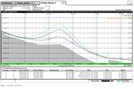
Figure 13 The phase noise with the same 3 regulators from Figure 8 compared to the results with a 2.4Ω and 33uF polymer electrolytic capacitor filter connected to the linear regulator. The addition of the R-C filter (red trace) nearly matches the best case “noiseless” voltage source (blue trace).
The calculated minimum capacitance and attenuation required for the switching regulator are included along with the simulated attenuation using a 2.4Ω resistor and an 82uF capacitor inserted between the voltage regulator and the clock. The simulation is performed at three different ESR values and the results are shown in Figure 14. Here we see that the higher noise of the switching regulator will require almost double the capacitance and significantly lower ESR to match the “noiseless” supply performance.

Figure 14 The required attenuation from Figure 10 (dots), minimum capacitor from Equation 2, and the simulated 2.4Ω and 82uF filter. Three ESR values are simulated, confirming the 70mΩ maximum ESR estimate.
The single pole R-C type filter is a simple, inexpensive, and effective solution for powering sensitive circuits from an inexpensive voltage regulator.
It is interesting that the switching power supply is quite noisy at frequencies of tens of kHz, while the switching frequency is much higher at 2.8MHz as noted in the measurement shown in Figure 15. This figure shows the 2.8MHz fundamental switching frequency and harmonics in the center trace and the noise with a 1kHz bandwidth in the lower trace.

Figure 15 Spectrum plots of the VRTS3 POL regulator show switching harmonics (middle graph) as well as broadband low-frequency noise (bottom graph)
The oscilloscope image in Figure 16 shows the switch node of the 2.8 MHz point of load (POL) regulator. In the bottom graph centered on the trigger at time 0, little leading-edge modulation is evident. The middle graph shows the waveform 60 uS after the trigger. Now both edges appear heavily modulated, indicating both pulse width and frequency modulation. This modulation, sometimes purposely added for EMI benefit to spread the spectral content and reduce peak amplitudes, results in low-frequency noise. This low-frequency noise ultimately establishes the size of the filter and not the switching ripple.

Figure 16 Switch node of the VRTS 3 POL regulator at 0us (trigger) and 62us after the trigger
High-frequency load noise can be combined with the noise filter by adding a ferrite bead or chip inductor with the series resistor. The maximum inductance value is related to the series resistor value and the filter capacitor:

Increasing the inductance value above this limit will result in spurious responses or increased noise. The maximum inductor value computed from Equation 4 using the 2.4Ω resistor and 33uF linear regulator filter is 95uH. Typically, this value will be lower and determined by considering the inductance, dc resistance (DCR), maximum operating current, and chips size. Because the total resistor required has not changed from the 2.4Ω value, the inductor DCR is subtracted from the 2.4Ω value, maintaining the same voltage drop and low frequency noise attenuation. Selecting an inductor with a 2.4Ω DCR completely eliminates the external resistor.
The TDK GLFR1608T470M-LR 47uH/35mA inductor is specified to have a 2.3Ω nominal DCR in a 0603 chip. The DCR of this inductor is close enough to the 2.4Ω so that no additional resistor is required and the filter does not occupy any additional PCB area compared to the resistor capacitor filter. The filter is shown schematically in Figure 17 and the simulated filter attenuation is shown in Figure 18.

Figure 17 A 47uH/2.3Ω chip inductor replaces the resistor maintaining the noise density and improving the high frequency attenuation and isolation.

Figure 18 The 2.3Ω DCR of the inductor satisfies the noise density attenuation while the inductance greatly improves the high frequency attenuation. The inductance is below the maximum value; therefore, there is no peaking in the filter.
The low-frequency noise attenuation is provided entirely by the resistor. Removing or reducing it will increase the clock noise and will also result in peaking. The capacitor ESR is fixed at 5mΩ and the DCR of the 47uH inductor is swept from 0.3Ω to 2.3Ω. The results shown in Figure 19 show this clearly. Reducing the resistance to 1.3Ω fails to provide the required 6dB attenuation at 5kHz and reducing it further to 0.3Ω results in 11dB gain at 4kHz.

Figure 19 The 47uH filter resistance is stepped from 0.3Ω to 1.3Ω and 2.3Ω while maintaining the 33uF capacitor with a 5mΩ ESR. At 1.3Ω the filter fails to provide the necessary noise density attenuation of 6dB at 5kHz.
The allowable power supply noise density can also be calculated directly from the phase noise measurements of the “noiseless” source versus the linear and switching regulators shown in Figure 10. Subtracting the 6dB phase noise degradation at 5kHz from the -12dBuV/√Hz linear regulator noise results in a tolerable noise of -18dBuV/√Hz at 5kHz. Similarly, subtracting the 14dB phase noise degradation from the -4dBuV/√Hz switching regulator noise also results in an allowable voltage noise of -18dBuV/√Hz.
High-Accuracy Low-Noise Regulators
There are high-accuracy voltage regulators designed for sensitive applications. Examples include the Linear Technology LT3042 and the Analog Device ADM7154. A block diagram of the ADM7154 is shown in Figure 20. The voltage reference is generally the dominant noise source in the voltage regulator and so the reference buffer is brought out to a pin for external capacitance to reduce the power supply noise. The amplifier to the opamp and driver supplies are also sensitive, so that bypass pin is also brought out for external capacitance to reduce the power supply noise. The input to the regulator MOSFET is also brought out to a VREG pin so that external capacitance can be connected to reduce noise. The complete application circuit is shown in Figure 21.

Figure 20 Block diagram of the Analog Devices ADM7154 obtained from the manufacturers datasheet
This circuit requires five capacitors to minimize the voltage regulator noise. In most cases, the passive filtering of a lower cost regulator will perform just as well at a small fraction of the cost. This is especially true given that most sensitive circuits are sensitive to voltage noise, but generally do not require the absolute voltage level to be extremely accurate.

Figure 21 The typical application circuit for the ADM7154 shows 3 external filter capacitors in addition to the input and output filter capacitors.
Conclusion
The addition of a simple R-L-C filter to the output of a regulator can provide a low-cost solution to achieving the ultra-low noise supply for power-sensitive circuits. The required level of noise reduction can be obtained from a measurement of the sensitive circuit using the voltage regulator of choice compared to a measurement using a “noiseless” power supply or line injector. Simple calculations for the R, L, and C values can be used and then simulated to verify the desired noise attenuation versus frequency.
Measured results confirm the low noise floor of a linear regulator with an output R-C filter. Additional high frequency attenuation to further reduce load noise can be achieved by replacing the resistor with an inductor that includes the desired DCR.
It is possible to simulate the impact of power supply noise on phase noise and time jitter using a large signal simulator.
Paying for specialized low-noise regulators may not be necessary if one is interested in low noise and not absolute voltage accuracy. The low-noise regulators still require numerous external capacitors, and may not actually reduce the part count when compared to a simple L-C filter with engineered DCR and ESR.
Appendix: Design Tips
There are a few ways to improve your first-pass design success rate.
Include power supply noise as well as any interconnecting wire inductance and input capacitors, especially if the power supply is external as in a bench power supply.

Figure 22 Be sure to include power supply noise and interconnecting wire inductance and input capacitance. In some cases, the capacitance is internal as in a crystal oscillator. Measure the impedance at the input pins if you are not sure.
Figure 23 Oscillator phase noise with (blue) and without (red) power supply noise included. Note the elevated noise floor in addition to the clear noise that is from a resonant input interconnecting cable.
The simulator can also interpret timing jitter from a phase noise simulation and markers can be used to limit the integration bandwidth.
Most datasheets and specifications refer to jitter rather than phase noise. Although I prefer phase noise because it provides the frequency data, the two are directly related, allowing the simulator to transform one to the other as shown in Figure 24.

Figure 24 The simulator calculates the area under the curve from between marker f_low and f_high and transforms the phase noise to time jitter
Not all voltage regulators are created equal. Measure a large variety.
I like to mount voltage regulators to small daughter cards that I can plug into a carrier board as shown in Figure 25. This allows quick, accurate, and repeatable measurements and can also include an interconnect for the sensitive circuit. The variation from one voltage regulator to another can be 20 dB or more. Voltage regulators with poor stability will also show resonant peaks similar to the peak seen in Figure 23.

Figure 25 A carrier board with voltage regulator daughter boards makes it simple to measure a large sample of voltage regulators quickly.
Voltage regulators have several noise paths, including air.
The voltage regulator has several noise sources, not just output noise. Some percentage of noise at the input of the voltage regulator will leak through to the output determined by the power supply rejection ratio (PSRR). Choosing a regulator with a high PSRR will reduce the external filtering. The output impedance also propagates noise due to current noise for the sensitive circuit. Measure the impedance at the operating load current and look for output impedance that is low and flat. Long, unshielded traces or resonant circuits will be sensitive to nearby EMI. Keep the sensitive circuits as far away as possible from switching power supplies or shield them. As in the previous note, make sure the impedance is low and flat at the sensitive circuit input.
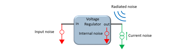
Figure 26 The voltage regulator has many noise paths to consider and not just the output noise.
Connecting a near field probe to a wideband harmonic comb is the quickest and simplest way to turn up resonances, as seen at the lower right corner of the screen in Figure 26.
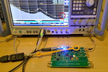
Figure 27 A harmonic comb connected to a near-field is a quick way to locate resonances in the power connections.
References
[1] Alan Walsh, “Voltage Reference Design for Precision Successive-Approximation ADCs.” http://www.analog.com/en/analog-dialogue/articles/precision-successive-approximation-adcs.html
[2] Walt Jung, “Build an Ultra-Low-Noise Voltage Reference.” Electronic Design Analog Applications Issue, June 24, 1993.
[3] Steven M. Sandler, “The Inductive Nature of Voltage Control Loops.” http://www.edn.com/electronics-blogs/impedance-measurement-rescues/4438578/The-inductive-nature-of-voltage-control-loops
[4] Steve Hageman, “Simple Circuits Reduce Regulator Noise Floor.” http://www.edn.com/electronics-blogs/the-practicing-instrumentation-engineer/4422750/3/Simple-circuits-reduce-regulator-noise-floor
[5] Steven M. Sandler, “Troubleshooting Clock Jitter and Identifying PDN Sensitivities.” https://www.eeweb.com/blog/eeweb/troubleshooting-clock-jitter-and-identifying-pdn-sensitivities
Author(s) Biography
Steve Sandler has been involved with power system engineering for nearly 40 years. Steve is the founder of PICOTEST.com, a company specializing in power integrity solutions including measurement products, services, and training. He frequently lectures and leads workshops internationally on the topics of power, PDN, and distributed systems and is a Keysight certified expert for EDA software.
He frequently writes articles and books related to power supply and PDN performance and his latest book, Power Integrity: Measuring, Optimizing and Troubleshooting Power-Related Parameters in Electronics Systems, was published by McGraw-Hill in 2014.