As data center systems evolve to support increasingly demanding artificial intelligence (AI) and machine-learning (ML) workloads, maintaining signal integrity at 224 Gbps PAM4 has become a major architectural challenge. One of the primary limitations is insertion loss in conventional PCB traces, which increasingly constrains performance as data rates rise. This paper explores a co-packaged interconnect approach that addresses this limitation by placing the high-speed separable interface directly on the package substrate. By moving away from traditional mid-board layouts and using compact substrates of approximately 95 mm × 95 mm or smaller, the design substantially reduces loss in the signal path.
The paper presents the architectural rationale and a detailed electrical evaluation of an electrically pluggable solution. The platform supports co-packaged copper for short-reach connections and co-packaged optics for longer distances, all within a common connector footprint. Measurement results and 3D electromagnetic simulations show strong 224G performance for high-density interconnect (HDI) PCBs. Overall, the approach provides a practical path toward scalable 102.4T/204.8T systems and future 448G designs.
The 224G Inflection Point is Architectural
The transition to 200G/lane and 224G electrical signaling is no longer only a roadmap discussion. IEEE P802.3dj is in the latter stages of the 200 Gbps, 400 Gbps, 800 Gbps, and 1.6 Tbps Ethernet project [Draft 3.1 at the time of writing], and OIF CEI-224G implementation agreements separate the electrical problem into very-short reach (VSR), medium reach (MR), long reach (LR), and linear application spaces.1-3 That segmentation is important because it reflects what system designers already see in practice: no single channel architecture can efficiently cover every reach, density, and serviceability requirement.
For 224G PAM4, the unit interval is 8.93 ps and the electrical Nyquist frequency is 56 GHz. 224G studies have shown why this is difficult: passive electrical performance often degrades rapidly above ~45 GHz, while high SerDes I/O density leaves little room for generous escape routing. With a bump-to-bump loss budget of no more than 32 dB at Nyquist for a high-density 224G VSR PAM4 networking system, the package, board, cable, and connector must be studied together to create a coupled budget rather than treated as independent degrees of freedom.4
The implication is straightforward. If the escape topology consumes too much loss and return loss margin before the signal reaches the cable or optical engine, the rest of the channel must be nearly ideal. At 224G, the most valuable signal integrity improvement may come from removing a lossy structure rather than further optimizing it.
Design Example: Where the Escape Budget Goes
A representative design example illustrates why topology matters. Consider a 100 mm × 100 mm package with a 50 mm × 50 mm die and approximately 1024 high-speed differential-pair resources. If corner-directed escape pushes a lane to roughly 45 mm of package routing, a 0.189 dB/mm package-loss assumption consumes ~8.5 dB of loss at 56 GHz before the signal reaches the board. Previous work has cited a more aggressive package trace-loss target near 0.123 dB/mm at Nyquist to enable as much as 60 mm of total TX-plus-RX package routing, together with a package vertical-loss target around 1 dB and BGA pitch at or below 0.8 mm.4 The exact value depends on substrate technology and routing rules, but the architectural lesson is independent of the specific stackup: long package escape is expensive.
Figure 1 uses representative channel data for a 300 mm path at 56 GHz. A package-mounted copper (co-packaged copper; CPC) channel is approximately -14.4 dB, while a near-chip connector (NCC) cable topology that still retains package-to-board and PCB breakout structures is approximately -19.0 dB. That 4.6 dB difference is large enough to change equalization stress, reach, retiming pressure, or manufacturing margin. The important point is not that any one cable is ideal; the improvement comes from removing the most loss-dense portions of the escape path before the signal reaches the controlled interconnect.
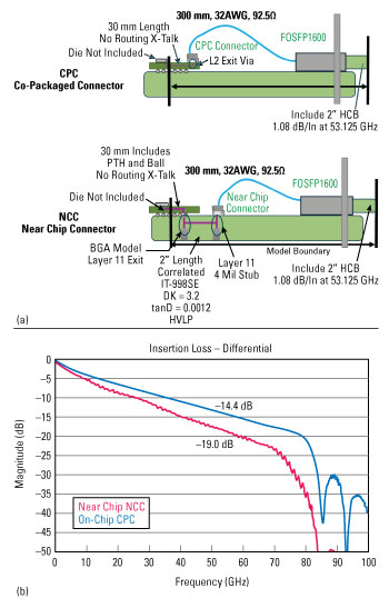 Fig. 1 Conventional package-to-board escape (NCC) versus package-mounted copper escape (CPC). The conventional path includes package substrate, BGA or socket, PCB breakout, via field, host trace, connector launch, and cable. The package-mounted path transitions directly from substrate to controlled twinax.
The loss-density comparison in this example is intentionally simple: package routing is treated as roughly 0.189 dB/mm at 56 GHz, PCB routing as roughly 0.063 dB/mm, and controlled twinax as roughly 0.014 dB/mm. These are representative design values, not universal material constants. They show why a millimeter inside the package or board is much more expensive than a millimeter in well-controlled cable.
Co-Packaged Copper
CPC places the high-speed separable electrical interface directly on the package substrate. The twinax cable is not lossless, but it is a better controlled and larger copper cross-section medium than long package and PCB routing for high-speed links. The benefit comes from eliminating package-to-board transitions, PCB breakout, via fields, and connector launches from the highest-speed portion of the channel.
In practical 224G terms, several recovered “dBs” can be used for additional reach, lower transmitter or receiver equalization stress, improved production margin, or reduced dependence on active retiming. The improvement is architectural: the channel is not saved by making copper ideal, but by moving the controlled cable closer to the SerDes.
This direction is consistent with beyond-200G research. A DesignCon 2025 paper on the path toward 400G/lane argued that traditional ASIC-PCB-connector-module topologies are unlikely to support future 400+G channels using familiar channel metrics and identified silicon-to-twinax and other alternative architectures as likely requirements.5 For 224G systems, the same reasoning applies earlier: when the board path is the problem, the cleanest answer is often to use cable, as much of it as possible.
Connector Density and HDI Routing Are Distribution Problems
Connector density should not be evaluated only as a mechanical placement issue. At 224G, it also controls the distribution of loss, skew, return loss, and crosstalk across the lane population. A lower-density connector can appear easier to route yet still produce a worst-case lane if added rows force long detours around the connector field.
The design target should, therefore, be the full lane distribution rather than only the nominal lane. An HDI topology with slightly higher typical loss but a much tighter tail can be easier to equalize, train, test, and manufacture than a topology with a few long, lossy outliers (see Figure 2).
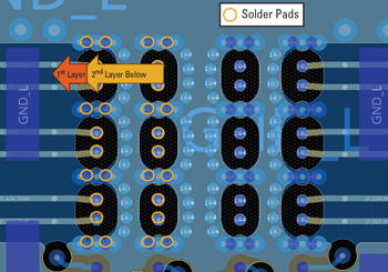 Fig. 2 HDI escape for dense co-packaged connectors. Terminated microvias and HDI layers (indicated by orange arrows) reduce detours and narrow lane-to-lane loss variation relative to row-wise non-HDI breakout.
Copper Remains Valuable Until Geometry Becomes the Limit
Co-packaged copper is well matched to short, passive, latency-sensitive scale-up links: tray-to-tray, blade-to-blade, orthogonal-board, or local rack architectures where the channel budget can close without the need to retime the signal. Passive copper cables can reduce energy and latency because long PCB equalization burden as well as unnecessary optical conversion are avoided. Copper, however, does not scale indefinitely. At high radix, the limiting variables become package edge length, top-side attach area, cable bend radius, retention hardware, power-delivery access, thermal keep-outs, and serviceability.
The 204.8T scaling case illustrates the geometry limit. At 224 Gbps per lane, 204.8T corresponds to roughly 1024 serial lanes. Counting transmit and receive physical resources separately, a total of 2048 differential pairs are required. With 64 differential pairs per package-mounted copper connector, the package requires 32 connectors. Given reasonable die sizes for these lane counts and the area required to fit 32 connectors, reducing the package size below 120 mm × 120 mm becomes extremely difficult.
This is the practical copper-to-optics boundary. The channel may still be electrically possible, but the package can become dominated by connector beachfront, mechanical constraints, and cost. Some longer package traces may also become too loss-dominated for passive copper, driving the need to consider alternative technologies.Migration-Ready Package Interfaces
A useful next step is a common package-level interface that supports either passive co-packaged copper or an optical engine. In this article, CPC refers to a co-packaged copper implementation, while CPX (see Figure 3) refers to the broader migration concept for co-packaged copper or co-packaged optics (CPO). CPX is, therefore, a shared high-speed package interface for the data path with a secondary floating connector or equivalent interface for optical-engine power, management, sideband control, and module identification.
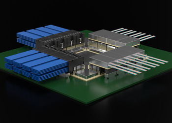 Fig. 3 Migration-ready package interface. One high-speed package interface can support passive twinax copper or an optical engine; optics add secondary power, management, and sideband interfaces.
This approach matters because different links cross the copper-to-optics boundary at different times. Short scale-up links may remain passive copper. Longer rack-level paths, higher-radix switch fabrics, or denser optical fanout may require near-package optics or co-packaged optics. A common interface preserves mechanical and electrical validation leverage across SKUs and generations instead of forcing a redesign of the package, board, thermal solution, and cable plant each time the medium changes.
OIF CEI-224G-Linear points in the same direction. The project targets full linear optical modules for Ethernet, UEC, and AI/ML applications with lower power, cost, complexity, and latency, and identifies electrical interfaces intended to support linear pluggable optics (LPO), CPO, and near-package optics (NPO) use cases.3 Linear optics remove or reduce digital signal processing (DSP) isolation in the optical module, so the host electrical channel becomes more important. Note that a poor package escape can give back the power and latency that the linear optical architecture was meant to save. The Open CPX MSA also reinforces the industry desire for a common mechanical, thermal, electrical, optical, and management interface for co-packaged and near-package AI data center interconnects.6 With a bump-to-optical-engine-to-bump loss budget of 18 dB at Nyquist, a co-packaged connector becomes necessary for 200T-class, large-radix packages.
A common socket for both copper and optics enables a standard platform that can use either medium depending on the end use case; critically, that decision can be made during or after system installation. Electrically pluggable optics also provide test and reliability advantages, making the common-interface approach a compelling design choice.
An electrically pluggable optical socket also raises the possibility of NPO instead of CPO for very large-radix devices. Moving to NPO can reduce package size and recover significant reach. It also raises the question of whether lower-density connectors are better for NPO because they allow more relaxed PCB design rules. As in the co-packaged case, however, that assumption may not hold.
Consider a representative case with the following assumptions, all at Nyquist:
- Package loss: 5 dB
- PCB loss: 0.063 dB/mm
- Differential-pair channel size: 0.5 mm (line + space + line)
- Connector choices: 32-lane connector/engine or 16-lane connector/engine.
Figure 4a and Figure 4b show connector and engine placements that allow all connector differential pairs to be routed to the ASIC using good signal integrity practices. Figure 4c shows the difference in minimum and maximum loss from the ASIC to the closest and farthest differential pairs for each case. While the minimum loss is similar in both cases, the 32-lane connector enables a 32-lane optical engine, allowing more channels to be placed closer to the ASIC. This results in a much lower loss spread for the denser connector case.
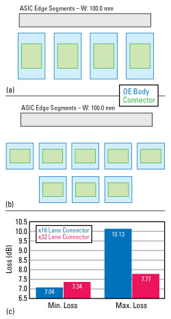
Fig. 4 Impact of connector density on the loss to route from the ASIC to the optical engine.
Optics Solve Density and Reach, but They Move the Engineering Burden
Near-package and co-packaged optics shorten the high-speed electrical path and improve bandwidth density, but they move complexity into the optical, thermal, manufacturing, and service domains. Laser strategy, fiber attach, optical test, module replacement, field repair, as well as reliability, availability, and serviceability all become architecture-level design topics.
Recent CPO system data show why the industry is interested. Broadcom has described a 51.2 Tbps Bailly CPO switch that integrates eight 6.4 Tbps silicon photonics engines with a Tomahawk 5 switch chip and claims 70 percent lower optical-interconnect power and an 8× silicon-area-efficiency improvement compared with pluggable transceiver solutions.7 Separately, an OCP/ECOC hyperscale evaluation reported stress-temperature reliability and optical-performance characterization for a 51.2T CPO switch system, including more than one million 400G-port device hours.8 These results are not generic guarantees for every CPO implementation, but they demonstrate that the question has moved from proof of concept toward deployable system qualification.
Validation Must Be Measurement-Driven and FEC-Aware
A credible 224G validation flow requires more than a smooth insertion loss plot from one typical lane. It should include package launch extraction, connector and cable models, de-embedding, time-domain reflectometry (TDR), return loss, NEXT/FEXT, mode conversion, skew, mate-cycle repeatability, thermal-mechanical sensitivity, link training, and post-forward error correction (FEC) error behavior. The package, connector, cable, optical engine, and FEC architecture must be reviewed as one system.
FEC is essential for PAM4 systems, but it is not free margin. DesignCon 2024 work on 200+ Gbps Ethernet FEC reviewed end-to-end, concatenated, and segmented FEC for multi-part electrical and optical links and noted that IEEE 802.3dj adopted Hamming (128,120) inner code as part of the 200G/lane IM-DD optics FEC solution.9 That matters for package-first interconnects because residual error statistics can differ among passive copper, LPO, NPO, CPO, and DSP-retimed optics. Burst behavior, training convergence, and interoperability should be evaluated with the physical channel, not after it.
Practical Design Rules
First, it is important to choose topology before optimizing details. If the signal is forced through long package routing, BGA escape, PCB breakouts, multiple vias, and a conventional front-panel launch, every element must be close to ideal. Direct package-to-cable or package-to-optics paths reduce the number of structures that require equalization.
Second, be sure to budget package edge length as carefully as insertion loss. Connector length, corner keep-outs, cable bend radius, power access, and cold-plate geometry should be included in the earliest channel-planning exercise. Third, optimize the lane population, not only the best lane. Fourth, use copper where copper is naturally strong: short passive links that benefit from low latency and low power. Finally, use optics where geometry, reach, or serviceable cable density dominates.
Conclusion
The 224G scale-up interconnect problem is not a copper-versus-optics argument. It is a placement problem: put each medium where it is physically and economically strongest. Co-packaged copper is compelling for short, passive, low latency links because it moves controlled twinax close to the SerDes and removes much of the package-to-board escape penalty. Near-package and co-packaged optics become necessary when reach, density, package beachfront, or system power dominate. A migration-ready package interface allows both approaches to coexist, reducing the risk that one generation’s copper solution becomes the next generation’s package redesign.
For practicing engineers, the shift is simple but consequential: we need to stop treating the package, PCB, connector, cable, optical engine, and FEC as separate optimization tasks. At 224G, and even more so at 448G, they are the channel. The winning architecture will be the one that spends the fewest high-loss millimeters before the signal reaches the medium best suited for the job