High-speed coaxial-to-grounded-coplanar-waveguide transitions are often optimized by adjusting planar launch parameters such as signal trace width, GCPW gap, and substrate geometry. However, the coaxial structure and its placement relative to the GCPW substrate can strongly influence the broadband response. This article begins with the same UT-20 coaxial-feedthrough-to-GCPW launch starting point used in previous AI-assisted optimization work1 and examines how coaxial conductor dimensions, top-side GCPW ground spacing, coax-to-GCPW lateral misalignment, and the coax-to-GCPW air gap affect the transition.
HFSS simulations compare S-parameters for several launch cases while the GCPW substrate stackup remains fixed. Poor alignment between the coaxial return structure and the planar grounds creates a less direct return-current transition, producing a local discontinuity and increased high-frequency reflection. The results also show that an axial air gap can reduce S21 even when S11 changes only modestly. The coax center conductor, coax outer conductor, GCPW signal trace, top-side grounds, air gap, and fixed ground-stitching structure must therefore be treated as one 3D launch.
Introduction
High-speed interconnect design often begins with familiar controlled-impedance elements. A coaxial connector or feedthrough is treated as a nominal 50Ω structure. A grounded coplanar waveguide (GCPW) is designed for the same impedance using trace width, gap, dielectric height, and ground geometry. In isolation, each structure may behave well. The difficulty is the transition between them.
At microwave and mmWave frequencies, this transition can dominate the interconnect response. The launch is not simply where the coaxial center conductor lands on the planar signal trace. It is a 3D electromagnetic conversion region in which both signal current and return current must move from a coaxial structure into a planar transmission-line structure.
The return-current transition is often the less visible part of the problem. In a coaxial line, return current travels on the inner surface of the outer conductor. In GCPW, it is distributed among the top-side ground rails, ground-stitching vias, and bottom reference plane. The launch must connect these return-current environments smoothly.
In previous work,1 an AI-assisted optimization approach was used to study a coaxial-to-GCPW transition by adjusting planar launch parameters including signal trace width, GCPW gap, and via geometry. The present article begins from the same starting point and examines what happens when the coaxial conductor dimensions, coax-to-GCPW placement, top-side ground spacing, and air gap are changed.
The GCPW substrate thickness and dielectric stackup are not varied. The focus is the coaxial interface and how that interface couples into the fixed GCPW substrate. Even when the planar geometry is controlled, the launch response can change if the coaxial outer conductor, center conductor, top-side grounds, or air gap alter the available return-current path.
The central argument is simple: a coaxial-to-GCPW launch should be designed as one 3D return-path conversion. The coax center conductor, coax outer conductor, GCPW signal trace, top-side grounds, air gap, and fixed ground-stitching structure form one electromagnetic system.
The Coaxial-to-GCPW Transition
In a coaxial transmission line, signal current travels on the center conductor, while return current travels on the inner surface of the outer conductor. This compact geometry keeps the signal and return currents tightly coupled.
A grounded coplanar waveguide has a different return-current structure. The signal trace is located on the top layer and is separated from adjacent top-side ground rails by a defined GCPW signal-to-ground gap. The bottom ground plane participates through dielectric coupling and nearby ground-stitching vias.
At the launch, the structure must transform a circular coaxial return path into a planar GCPW return path. When the coaxial outer conductor does not align well with the GCPW ground structure, return current must spread before it settles into the planar mode. This extended return path changes the local balance of inductance and capacitance, creating a localized impedance discontinuity.
The axial spacing between the coaxial interface and the GCPW substrate also matters. If an air gap exists, the signal and return paths must bridge an unsupported region before reaching the intended planar structure. This can add inductance, alter capacitance, and reduce high-frequency transmission.
The launch should therefore be evaluated not only by asking whether the coax center conductor lands on the correct signal trace, but also by asking how the coaxial outer conductor transitions into the complete GCPW ground system.
Simulation Approach
The simulated structure is a UT-20 coaxial feedthrough transitioning into a grounded coplanar waveguide. The GCPW includes a top-side signal trace, adjacent top-side ground rails, ground-stitching vias, and a bottom reference plane near the launch region.
The reference geometry is the same launch starting point used in the previous AI-assisted study.1 The intent is not to repeat that optimization or publish its exact dimensions. Instead, this article uses the same starting structure as a controlled reference and varies specific coaxial-interface and return-path features.
The GCPW substrate thickness and dielectric stackup are held constant. The variables are coaxial conductor geometry, top-side GCPW signal-to-ground spacing, lateral alignment between the coaxial structure and the GCPW launch, and axial spacing between the coaxial interface and the GCPW substrate.
Each case is evaluated in HFSS using S-parameters through 125 GHz. S11 magnitude is used to evaluate launch mismatch, while S21 magnitude identifies changes in broadband transmission and ripple. The port definitions, reference impedance, material definitions, boundary conditions, and frequency sweep are held constant so that the comparisons reflect geometry changes rather than simulation-setup changes.
Time-domain methods such as TDR can be useful for locating discontinuities in measured structures. This study, however, relies on HFSS S-parameters.
The launch-transition problem is examined using four simulation families:
- Coaxial conductor geometry, including outer-conductor and center-conductor dimensions
- Top-side GCPW signal-to-ground spacing
- Coax-to-GCPW lateral misalignment
- Coax-to-GCPW axial spacing, or air gap.
1. Reference Design
The simulated S-parameter response for the reference launch establishes the baseline broadband behavior before intentional transition changes are introduced. It provides a stable comparison point for evaluating coaxial conductor size, top-side ground spacing, lateral misalignment, and axial air-gap distance (see Figure 1).
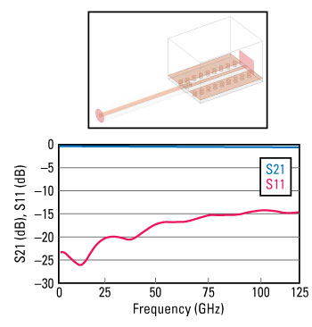 Fig. 1 Reference launch geometry and simulated reference S-parameter response.
2. Coaxial Conductor Geometry
The coaxial conductor geometry sweep is the central simulation family. The GCPW substrate and planar launch are held constant while the coaxial center-conductor and outer-conductor dimensions are varied.
The center conductor affects the signal transition into the GCPW trace. The outer conductor determines how the coaxial return path approaches the planar ground structure. A larger outer-conductor opening increases the distance between the coaxial return path and the top-side grounds. If the GCPW ground structure is not adjusted accordingly, the return path extends before entering the intended planar mode.
The outer-conductor inner diameter, defined as the opening surrounding the coaxial dielectric in the HFSS model, is swept from 12.5 to 30 mil. The center-conductor diameter is scaled proportionally in each case to preserve a nominal 50Ω coaxial impedance. The 17.5 mil case represents the UT-20 reference geometry (see Figure 2).
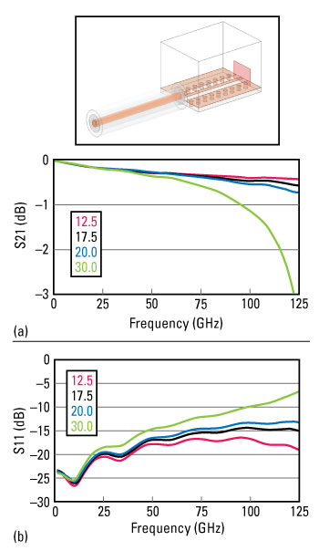 Fig. 2 Simulated S21 magnitude (a) and S11 magnitude (b) for the coaxial conductor geometry sweep. The outer-conductor inner-diameter cases are 12.5, 17.5, 20, and 30 mil, with the center conductor scaled to maintain nominal 50Ω impedance.
The results show progressively greater upper-band degradation as the coaxial dimensions increase. The 30 mil case produces the largest reduction in S21 and the weakest S11 performance. Reducing the coaxial dimensions below the UT-20 reference improves the simulated high-frequency transition, although center-conductor diameters below approximately 5 mil become increasingly difficult to fabricate, handle, and assemble.
3. Top-Side GCPW Ground Spacing
The top-side GCPW grounds provide the closest planar return path to the signal trace. Their spacing determines how quickly the coaxial return current can enter the planar ground structure.
This simulation family varies the GCPW signal-to-ground spacing from 4 to 12 mil while keeping the substrate stackup and coaxial geometry fixed. If the top-side ground edges are too far from the coaxial outer conductor or signal trace, the coaxial return path must travel farther before entering the GCPW mode. This can degrade S11 and S21, especially at high frequency (see Figure 3).
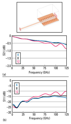 Fig. 3 Simulated S21 magnitude (a) and S11 magnitude (b) for GCPW signal-to-ground spacing of 4, 8, and 12 mil.
The results favor ground edges that align closely with, or extend inward from, the coaxial return structure. The 12 mil ground spacing produces the greatest high-frequency reflection and transmission degradation. The 4 and 8 mil cases avoid the same return-path extension and maintain the stronger broadband response.
4. Coax-to-GCPW Lateral Misalignment
This simulation family introduces lateral offset between the complete coaxial structure and the GCPW launch. The evaluated offsets are 0, 1, and 2 mil.
Misalignment affects both the signal path and the return path. Center-conductor offset changes the signal landing geometry, while outer-conductor offset changes the alignment between the coaxial return structure and the GCPW grounds. At higher frequencies, small offsets can degrade S11, reduce S21, and decrease assembly repeatability.
A 1 mil lateral offset produces only modest degradation relative to the aligned case. At 2 mil, the change becomes substantially more pronounced in both S11 and S21, particularly at the upper end of the simulated band. For this geometry, coax-to-GCPW lateral alignment should therefore be controlled to approximately 1 mil or better (see Figure 4).
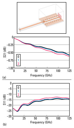 Fig. 4 Simulated S21 magnitude (a) and S11 magnitude (b) for coax-to-GCPW lateral offsets of 0, 1, and 2 mil.
5. Coax-to-GCPW Axial Spacing or Air Gap
This simulation family varies the axial air gap between the coaxial interface and the GCPW substrate. The evaluated cases are 0, 1, and 2 mil, representing realistic mechanical separation.
Increasing this spacing lengthens the exposed transition region before the signal and return paths reach the intended planar structure. The added unsupported length can alter the local inductance and capacitance and reduce high-frequency transmission.
This case is practical because the air gap may be established by housing geometry, substrate placement, solder attachment, feedthrough installation, or assembly tolerance. The sweep therefore tests how much unsupported spacing can be tolerated before the broadband response degrades (see Figure 5).
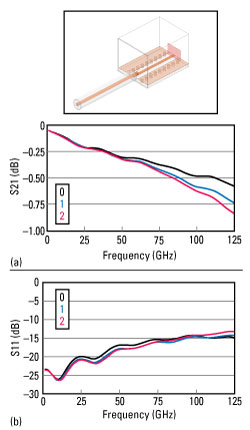 Fig. 5 Simulated S21 magnitude (a) and S11 magnitude (b) for axial air gaps of 0, 1, and 2 mil.
The air gap has relatively little effect on S11 over the simulated range, but S21 decreases progressively as the gap increases. The exposed transition length should therefore be minimized even when the input reflection appears acceptable. For this geometry, S11 alone does not fully reveal the performance penalty introduced by the air gap.
Design Implications
The coax center conductor, coax outer conductor, GCPW signal trace, top-side grounds, air gap, ground-stitching vias, and bottom reference plane form one electromagnetic transition (see Table 1).
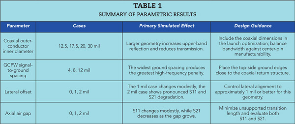 Parametric Case Descriptions and Results
The simulations support the following practical guidance:
- Treat the center conductor and return structure as a single 3D transition rather than only a center-pin landing on a nominally 50Ω trace
- Include the coaxial conductor dimensions in the electromagnetic optimization; nominally 50Ω coaxial structures do not necessarily produce the same launch response
- Position the GCPW ground edges to avoid extending the return-current path from the coaxial outer conductor
- Control lateral coax-to-GCPW alignment to approximately 1 mil or better for the geometry studied
- Minimize the axial air gap because acceptable S11 does not necessarily imply acceptable S21
- Evaluate both S11 and S21 when establishing mechanical assembly tolerances.
Conclusion
A coaxial-to-GCPW launch is a 3D transition between two different return-current environments. In the coaxial region, return current surrounds the center conductor. In the GCPW region, return current is distributed among the top-side ground rails, ground-stitching vias, and bottom reference plane.
When the coaxial and planar ground structures are poorly aligned, the return-current transition becomes less direct and high-frequency reflection increases. An axial air gap produces a different response in the cases studied: it changes S11 only modestly but progressively reduces S21 as the unsupported transition length grows.
The coaxial interface is therefore part of the broadband launch. Trace width, GCPW gap, and substrate stackup remain important, but they must be evaluated together with coaxial conductor dimensions, top-side ground placement, lateral alignment, and axial spacing. These variables can affect reflection and transmission differently, making both S11 and S21 necessary when evaluating the complete transition.
At high frequencies, the return path is not background metal. It is the other half of the launch.
REFERENCES
1. J. Yoho, A. Ramadurgakar, and M. Coopwood, “AI-Assisted HFSS Modeling For 100 GHz+ High-Speed Interconnect Design,” Signal Integrity Journal, Vol. 8, Issue 1, April 2026, pp. 6-10, Web: https://www.signalintegrityjournal. com/articles/4274.