
Power supply sections typically occupy a large proportion of a design’s real estate. Not only do they occupy a majority of space, but they critically impact the performance of the system.
Efforts to improve system level performance often require the improvement of the power system. These improvements, often considered the Figures of Merit (‘FOM’), come in the form of smaller circuits, operating at higher efficiency while generating lower system noise, including electromagnetic type noise (EMI), as well as output voltage noise.
Great strides have been achieved in GaN technology, which promises these FOM improvements. A great deal has been published relating to the evolving state-of-the-art for GaN on Si and GaN on SiC, most of it related to switching regulators. There are fewer publications relating to these devices in linear applications, such as LDOs.
Another area which has received little attention is the migration from Silicon power metal oxide field effect transistor (MOSFET) devices to Gallium nitride (GaN) high electron mobility transistor (HEMT) devices. In the 1980’s, technology began migrating from Bipolar Junction Transistors, which were the staple for power electronic switches, to MOSFET devices. The Si MOSFET devices offered many improvements, such as simpler drive requirements, lower on-state losses and much faster switching. The migration proved to be more difficult than might have been anticipated. The much faster switching of Si MOSFET devices promised lower switching losses, but there were also difficulties associated with the much higher di/dt the Si MOSFET presented. The leakage inductance of magnetics and relatively inductive printed circuit board planes allowed large voltage spikes which often caused device failures. Over time, engineers learned to design for the increased di/dt and Si MOSFET evolution has supported continuously improving performance. As we now approach the theoretical limits of Si MOSFET performance GaN promises to provide the path forward.
This paper is not about the improvements that GaN HEMT offers, as we have stated that much has been written on this topic. This paper address the migration path and the complexities that might be faced in attempting to migrate current state-of-the-art designs from the existing Si MOSFET devices to the current generation of GaN HEMT devices. This paper addresses both linear regulator technologies and switching regulator technologies, which each have their own migration paths and challenges.
GaN
Over the years, we have seen the evolution of power transistors using minority carrier bipolar junction transistor (BJT) devices progress to majority carrier based devices like metal oxide silicon field effect transistors (MOSFETs). The next big see-change seems to point to high electron mobility transistor (HEMT) GaN devices.
This section compares GaN to Silicon at both the material and device level. Only enhancement mode GaN (eGaN) device structures are considered in this paper, since this paper is focused on DC/DC VRMs and linear regulators.
Material properties
Some of the material properties of Silicon and GaN are listed [1] in the table below.
|
Parameter |
Silicon |
GaN |
|
Band Gap Eg (eV) |
1.12 |
3.39 |
|
Critical Field Ecrit (MV/cm) |
0.23 |
3.3 |
|
Electron Mobility µn (cm2/V.s) |
1400 |
1500 |
|
Permittivity εr (F/m) |
11.8 |
9 |
Table 1: Comparison of key material properties between Si and GaN
GaN is a higher band semiconductor, as its band gap voltage, Eg, is much higher than Si. This results in lower leakage current and higher operating temperature capability. Similarly, the critical field parameter, Ecrit, is much higher in GaN, resulting in higher drain-source breakdown voltage for an eGaN HEMT.
Aside from higher electron mobility, the permittivity and critical field parameters are factors that impact resistance, which is an important parameter driving conduction losses during power conversion.
Electrical characteristics
Electrical characteristics of the transistor are the aspects that affect the electrical performance at the circuit level. Some electrical characteristic [2], [3] performance comparisons are listed in the table and discussed below.
|
Parameter |
Silicon MOSFET (Infineon BSC060N10NS3G) |
eGaN HEMT (EPC2001) |
|
Leakage current |
1000 µA |
300 µA |
|
On-resistance |
6.6 mΩ |
5.6 mΩ |
|
Capacitance |
3700 pF |
850 pF |
|
Gate Charge QG |
51 nC |
8 nC |
|
Diode forward voltage, VSD |
0.8V |
1.75V |
|
Reverse recovery charge Qrr |
6.4 µC |
54 nC |
|
Reverse recovery time trr |
630 ns |
30 ns |
|
Transconductance Gfs |
85 S |
100 S |
|
Source-Drain Forward Voltage, VSD |
1 V |
1.75 V |
|
Threshold voltage change over temperature 250 to 1250 |
38% decrease |
3% increase |
|
Maximum Switching speed |
<1MHz |
100s of MHz |
|
Package size |
6.3 x 5.0 mm |
4.1 x 1.6 mm |
Table 2: Comparison of key electrical parameters between a 100V rated Si MOSFET and an enhancement-mode GaN HEMT
Breakdown voltage and leakage current:
Transistor breakdown occurs when the applied electric field exceeds the material parameter-critical field Ecrit. Since the Ecrit is higher for GaN as shown in table 2, the breakdown voltage, Vbr, tends to be higher for eGaN HEMTs.

 (1)
(1)
The higher breakdown voltages of eGaN HEMT allow an increased margin for overshoot conditions during switching transients.
Drain-to-source leakage current can cause increased power loss. As previously mentioned, eGaN HEMT devices have lower leakage current due to the higher band gap, Eg.
Threshold voltage:
The threshold voltage is the voltage below which the device is off. It is junction temperature dependent. Enhancement mode GaN (eGaN) HEMT devices tend to perform better in this regard. The Vth for the silicon device, for example, drops 38% when the temperature changes from 25 degrees to 125 degrees as compared to an increase of 3% for an eGaN device.
Gate drive voltage:
For eGaN HEMT, the nominal gate drive voltage is 5V, while the maximum rating is 6V. This leaves only 1V of margin. This is a tighter requirement compared to Si MOSFETs and requires damping of the gate-drive turn-on control loop.
And more importantly for migration, only a few currently available controllers have gate voltage outputs that are compatible with eGaN HEMT drive requirements.
On-resistance:
The on-resistance has a direct impact on the conduction loss. The on-resistance of eGaN HEMT is lower causing less conduction loss, Pcond, and delivering higher conversion efficiency.
 (2)
(2)
Capacitance and charge:
eGaN HEMTs can be portrayed as having gate-to-source, gate-to-drain, and gate-to-source capacitance as shown below. The capacitance is an important factor in determining the switching speed of the device and, therefore, the associated switching losses. The speed increases when the capacitance is reduced, as in the case of eGaN.
In addition to lower output capacitance, the gate charge required to turn on eGaN is lower, resulting in faster transition and switching rates. In our experiments of comparing the DRMOS vs eGaN LTC3891 boards, we noted that the driver operating current was 26mA for eGaN HEMT devices and 50mA for Si MOSFET devices, so this is one of the benefits of very low gate charge.
Apart from low gate charge, there is no reverse recovery charge, QRR=0,  in eGaN HEMT. Consequently, there is no reverse recovery power loss for eGaN based regulator designs, a significant benefit that increases power conversion efficiency.

Figure 1: eGaN transistor equivalent capacitance model
Radiation tolerance:
eGaN HEMT is inherently more radiation tolerant. For Si MOSFETs to be radiation hardened, the gate oxide needs to be thick and, therefore, trap a lot of charge, resulting in large shifts in parameters such as threshold voltage, which can result in field failures. Therefore, radiation-hardened Si MOSFETs tend to have lower switching frequency, lower efficiency, and larger size.
Packaging:
The size of an eGaN HEMT device is smaller than a Si MOSFET because of the smaller die size. Efficient packaging is also employed using the chip-scale LGA package. This results in a significant reduction in the overall size occupied by the eGaN HEMT on a printed circuit board (PCB). For example, in the table above, the area of an eGaN device is nearly 5 times smaller than a Si device.
Linear Regulators
Linear regulators are primarily used in applications, at lower operating current levels or those applications where voltage rail noise must be kept to a minimum. Since linear regulators generally present a higher output impedance than a switching regulator, these noise reductions are generally achieve via the lack of the switching ripple and associated spike noise. Improved power supply rejection ratio (PSRR) is also generally a benefit. However, the dynamic load current induced noise is generally higher for the linear regulator due to the higher impedance exhibited.
The significant FOM for the linear regulator include output impedance, dropout voltage (headroom), PSRR, and radiation sensitivity for some applications. Each of these FOM are considered in order to determine which device provides the better performance. Most are driven by the pass device, either Si MOSFET or eGaN HEMT. The requirements of the pass transistor are then considered in order to evaluate the migration path complexities that might be challenging.
The major design elements in linear regulators are the pass element, bandgap voltage reference, and error amplifier. The pass element transistor operates in the linear region.
|
Regulator FOM |
Key Pass Device Parameters |
Si MOSFET |
eGaN HEMT |
Winner |
|
Output Impedance |
Transconductance |
Lower |
Higher |
eGaN |
|
Dropout Voltage |
RDSon |
Higher |
Lower |
eGaN |
|
PSRR |
Junction Capacitance |
Higher |
Lower |
eGaN |
|
Noise |
Junction Noise |
Higher |
Lower |
eGaN |
|
Physical Size |
Electron Mobility Breakdown Field |
Lower Lower |
Higher Higher |
eGaN eGaN |
|
Radiation Tolerance |
Radiation Hardening |
Not Hard |
Hard |
eGaN |
|
Junction Temperature |
Rtheta |
Lower |
Higher |
Si |
Table 3: Comparison of figures of merit between Si MOSFET and enhancement-mode GaN HEMT linear regulator designs
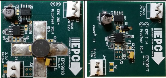
Figure 2: Picotest/EPC linear regulator boards: Si RF BJT (left) and eGaN HEMT (right)
The Discrete Linear Regulator Migration Path for Existing Designs
In the case of a discrete linear regulator, the migration path for an existing design is very simple and there are only a few concerns.
- The gate source voltage must be kept below 5V or the eGaN HEMT device will be damaged
- Only N-channel designs can be migrated as there are no P-channel eGaN HEMT devices.
- There must be sufficient cooling to account for the higher thermal resistance resulting from the smaller size of the eGaN HEMT device.
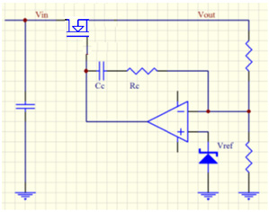

Figure 3: Typical Discrete Linear Regulator circuit schematic representing common topology for both Si and eGaN devices
Each of the figures of merit are considered [4] for the discrete linear regulator.
Output impedance

And the output impedance model can now be represented as shown in Figure 4.

Figure 4: Output impedance model of linear regulator
These results clearly show that even without increasing the bandwidth, which eGaN HEMT would allow, all three terms have Gfs in the denominator and so all are improved by the migration from Si to eGaN within an existing design. The benefits of the lower output impedance are directly reflected in the system performance. The measurements in figure 5 show greatly reduced clock phase noise using a lower output impedance eGaN HEMT voltage regulator compared with a typical linear regulator.

Figure 5: Comparison of measured phase noise of clock powered by linear regulators, Si LM317 (dim memory trace) vs eGaN (bright data trace)
The control loop bandwidth, GBW, can be significantly increased by replacing the control opamp or in some cases by tailoring the frequency compensation. Either of these would further improve the PSRR.
An example of two regulators, one using a BJT pass device and one use an eGaN HEMT pass device is shown in Figure 6 below.
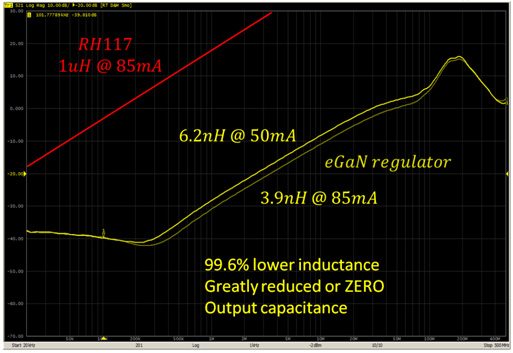

Figure 6: Comparison of measured output impedance benefit from higher bandwidth Si three terminal regulator (Red trace) vs eGaN (yellow traces)
Physical size
The eGaN HEMT device output impedance is lower. This means that less external output capacitance is required to maintain stable performance. Such smaller external capacitance requirement can be met easily with smaller size capacitors. This can further reduce the overall physical size of the regulator circuit.
The output impedance seen at the regulator output is low and its frequency response is equivalent to that of a 3.9nH inductance, which is the bare minimum considering the fact that the ESL of a tantalum capacitor is around 3.9nH. This shows that no additional inductance is being added by the eGaN HEMT that needs to be compensated by external capacitors, resulting in smaller overall size of regulator circuit.
Lower noise
Regulators with lower impedance result in the lower noise in the circuits they power. For example, a reduced impedance regulator yields lower noise clocks as shown the Figure 5 above.
Dropout voltage
The dropout voltage, also known as headroom, is the minimum voltage drop across the regulator as it delivers the load current and it can be represented as,
 (8)
(8)
As eGaN offers lower RDSon, the dropout voltage performance is improved as a result of replacing the existing Si MOSFET device with an eGaN HEMT device.
Power supply ripple rejection ratio (PSRR)
AC voltage fluctuations presented at the input to a regulator result in corresponding noise at the output. PSRR is a measure of the ability to reject such input variations.
 (9)
(9)
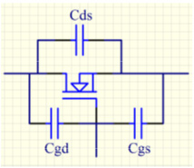
Figure 7: eGaN transistor equivalent capacitance model
Since eGaN HEMT offers significantly reduced junction capacitance compared to Si MOSFET, the PSRR performance is directly improved. Again, the control loop bandwidth can be significantly increased by replacing the control opamp or in some cases by tailoring the frequency compensation. Either of these further improve the PSRR.
To sum up linear regulator migration, it is evident that the migration of discrete linear regulators from Si MOSFET to eGaN HEMT is simple, with multiple FOM significantly improved. The considerations are only whether there is adequate cooling for the eGaN device and whether the gate is protected so that the eGaN gate-source voltage limit is never exceeded. In many cases, the control loop bandwidth can easily be increased, allowing additional performance improvement. It is also often possible to reduce the output capacitance, reducing cost and weight while improving reliability of the existing design. In applications where a radiation tolerant MOSFET is used the cost savings can be substantial.
Switching Regulators
Switching regulator circuits are found in many applications, suited primarily for those at higher operating current levels or those applications where efficiency is paramount and the voltage difference between the input and output is high. Large step-down ratio converters, for example, are often implemented as switching regulators. Since switching regulators generally act as point of load regulators for high speed devices, low output impedance over a wide band of frequencies and faster transient response is desired. Since switching regulators operate by turning the transistors on and off periodically, voltage and current ripple are generated at the input and output and are more noisy than linear regulators.
The significant FOM for the switching regulator include efficiency, transient response, and signal integrity of switch node waveforms. Each of these FOM are considered against the Si or GaN switch device parameters in order to determine which device provides the better performance. The requirements of the switch transistor are then considered in order to evaluate the path of migration and complexities that might inhibit such migration.
The major design elements in switching regulators are the main high side control switch, synchronous low side rectifier switch, gate controller, output inductor and capacitor filters. The switch element transistors operates in the saturation region.
|
Regulator FOM |
Key Switch Device Parameters |
Si MOSFET |
eGaN HEMT |
Winner |
|
Efficiency |
RDSon, Reverse conducting body diode, Package inductance, capacitance |
Lower |
Higher |
eGaN |
|
Gate drive voltage overshoot tolerance |
Gate drive voltage margins |
Lower |
Higher |
Si |
|
Layout parasitic impact on performance |
Gate drive voltage margins |
Lower |
Higher |
Si |
|
Temperature range |
Temperature coefficient of RDSon and Vth |
Lower |
Higher |
eGaN |
|
Switch node waveform |
Electron Mobility Breakdown Field |
Lower Lower |
Higher Higher |
eGaN eGaN |
|
Gate charge, Capacitance |
Gate charge, capacitance |
Slower (<1MHz) |
Faster (100s of MHz) |
eGaN |
|
Size |
Package, need for external components |
Bigger |
Smaller |
eGaN |
Table 4: Comparison of the figures of merit between Si MOSFET and enhancement-mode GaN HEMT based switching regulator designs

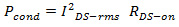
Figure 8: 12 to 1V switching regulator boards: first row is top view & the second is bottom view
The Discrete Switching Regulator Migration Path for Existing Designs
In the case of a discrete switching regulator, the migration is not trivial and there are several concerns when migrating an existing design.
-
The eGaN HEMT does not have a body diode that is formed in a manner similar to the Si MOSFET’s pn junction. However, the eGaN HEMT conducts similarly to the diode but with a higher voltage drop of 2V instead of 1V. This causes higher losses during the reverse conducting dead times. To provide an efficient path for reverse conduction current during the dead time, an external Schottky diode needs to be added. Another important design concern is to configure the gate controller to have as low a dead time as possible. The lower the dead time, the less reverse conduction flow there is, thereby achieving higher conversion efficiency.
-
The gate-source voltage must be kept below 5V or the eGaN HEMT device will be damaged. Most current gate controllers support higher gate drive voltage upwards of 7V. When migrating a design, such voltages need to be level shifted to 5V. In the migrated design figure below, the reverse biased Zener diode does this function of gate level shifting to 5V.
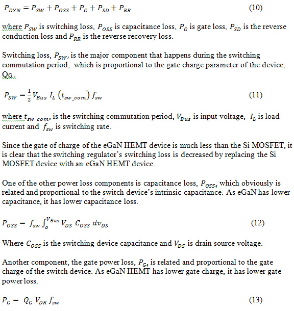
- eGaN HEMT is susceptible to board layout parasitics. Compared with Si MOSFET, eGaN HEMT runs at much higher di/dt and dv/dt rates, making it vulnerable to corresponding Ldi/dt and Cdv/dt spikes. Such overshoots at the gate drive can exceed the recommended 6V of eGaN HEMT, potentially damaging the device, as shown in the Figure 10 below. Also, overshoot voltages incur power loss. Therefore, the PCB board layout needs to be optimized for suitable eGaN performance.
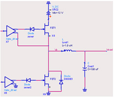

Figure 9: Typical discrete switching regulator circuit schematic
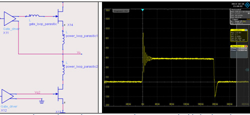
Figure 10: Gate loop and power loop parasitic inductances are highlighted in schematic; The higher speed eGaN devices can create significant ringing on the drain voltage which generates EMI and increases voltage stress.
The key figures of merit are considered for the discrete switching regulator.
Efficiency
The switching regulator power conversion efficiency depends on the dynamic power losses that occur during the transition of transistors from on to off and vice-versa. The dynamic power loss, consists of many components. Switching loss is due to the transient currents. Other losses include: output capacitance loss that is associated with the charging and discharging of intrinsic output capacitance of transistor; gate charge loss is the energy dissipated to charge the gate; reverse conduction loss that occurs in the low side transistor during the dead time; and reverse recovery loss that happens when the body diode transitions from the on-state to off-state.
Where  is the gate charge.
By comparing the losses from the table below, we can note that the total loss is lower in eGaN device based switching regulator, provided the conduction loss is controlled.
|
Regulator Losses |
Key Switch Device Parameters |
Si MOSFET |
eGaN HEMT |
Winner |
|
Switching loss |
Gate charge |
Lower |
Higher |
eGaN |
|
Reverse conduction loss |
RDSon |
Higher |
Lower |
Si |
|
Capacitance loss |
Gate drive voltage margins |
Higher |
Lower |
eGaN |
|
Reverse recovery loss |
Temperature coefficient of RDSon and Vth |
Lower, nearly zero. |
Higher |
eGaN |
|
Gate charge loss |
Gate charge |
Lower Lower |
Higher Higher |
eGaN eGaN |
Table 5: Comparison of power losses between Si MOSFET and enhancement-mode GaN HEMT switching regulators
Physical Size
With the migration to eGaN HEMT, the smaller eGaN HEMT device package results in reduction of regulator’s physical size, provided the heat dissipation is handled. Another aspect that could improve the size reduction is simplifying the filter components-inductor and capacitor- by increasing the switching frequency. The eGaN HEMT device output impedance is lower and this means that less external output capacitance is often required to maintain a low impedance and stable performance. This can further reduce the physical size of the regulator circuit and save cost.
Switch node waveform
Measuring the switch node voltage is the most basic measurement for a power switch. This is typically measured from the drain-to-source of the device.
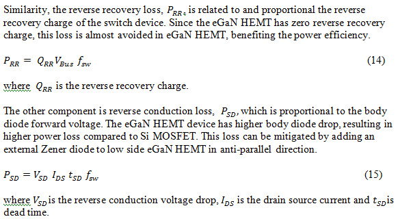
The fast switching of eGaN reveals many measurement challenges [5][6]. The switch node waveforms for eGaN vs. Si based regulators are compared in the measurements of the DRMOS and eGaN boards. The eGaN waveform are found to have sharper transitions.
Given the voltage step down specification of 12V to 1V, a Si MOSFET based switching regulator board- Fairchild DR MOS regulator was migrated to EPC eGaN HEMT based. The following measurements were performed on these boards.
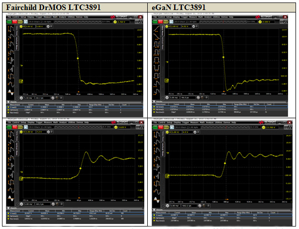
Figure 11: Switch node waveform comparisons: Si MOSFET and eGaN HEMT based regulators
Gate drive voltage stability
The gate drive waveforms for eGaN HEMT based regulators vs. Si MOSFET are compared in the measurements of DRMOS and eGaN LTC3891 test boards. For eGaN HEMT, it is important to verify that the PCB layout parasitic inductance is minimized in order to keep the gate voltage under designated limits. The measurements below show that the gate voltage on the eGaN LTC 3891 regulator is contained below 6V, the maximum allowed gate voltage.
Figure 12: Gate drive waveforms comparison: Si MOSFET and eGaN HEMT based switching regulators
EMI
EMI measurements on the Si MOSFET and eGaN HEMT test boards from figure 8 are shown here. The measurements are uncalibrated using either H-field or E-field probes close to the board and placed as noted in the figures. A telescopic antenna approximately 3 feet from the test board is also included for each boards. The telescopic antenna is shown in Figure 13 below.
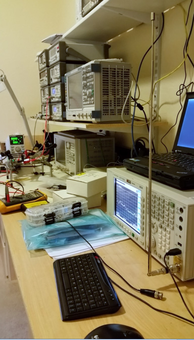

Figure 13: Test setup showing telescopic antenna connected at Spectrum analyzer
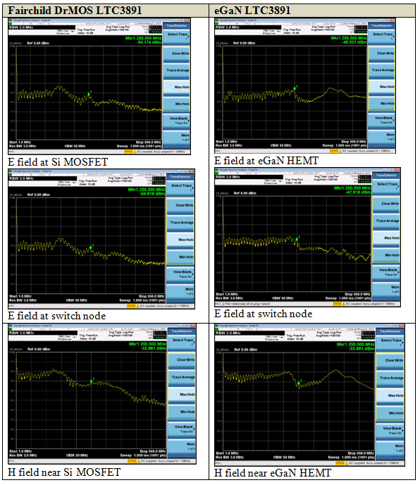

Figure 14: Emission from switching regulator boards: Si MOSFET and eGaN HEMT based
As shown in the figure 14 above, the emissions are quite different for the eGaN HEMT and Si MOSFET devices, especially at the higher frequency. The eGaN device is expected to have more high frequency signal due to the faster edge speed. The result is that the EMI filtering and screening requirements are likely different for eGaN HEMT and Si MOSFET presenting another challenge for the migration of existing designs.
To summarize, it is clear that the migration of discrete switching regulators from an existing Si MOSFET design to eGaN HEMT is not trivial. The migration is challenging because the majority of the present day controllers have gate drive voltages that exceed eGaN ratings and existing controllers also have long dead times where the reverse conduction of eGaN HEMT is lossy, eroding the efficiency benefits of eGaN HEMT. The EMI filtering requirements and PCB decoupling requirements are also different for the eGaN and Si devices. In general, the design has to be eGaN HEMT specific in order to take full advantages of the eGaN device benefits: higher switching rates, power conversion efficiency and faster transient response.
Conclusion
We have set out to explore the potential for migrating existing linear and switching type Si MOSFET based designs to eGaN HEMT technology. We have shown that existing linear regulator designs can directly benefit from replacing the Si BJT or MOSFET with eGaN HEMT. We have also shown that as part of this migration it is also possible to increase the operating bandwidth of the regulator further improving the performance.
The migration of switching designs from Si MOSFET to eGaN HEMT is complex and we cannot take full advantage of eGaN technology simply by changing the switches from Si to eGaN. For switching regulators, it is generally necessary to design it for eGaN from the start. The eGaN design offers great performance improvements, though this improvement necessitates careful design of the gate drive, dead time, PCB decoupling and EMI filtering to optimize the benefit. Such an optimized eGaN HEMT based switching regulator design will outperform a Si MOSFET based solution in most cases.
References
[1] “GaN Transistors for Efficient Power Conversion”, Alex Lidow, Johan Strydom, Michael de Rooij, David Reusch
[2] Infineon BSC060N10NS3G - N-ChannelSi MOSFET data sheet
[3] EPC2001 - Enhancement Mode GaN Power Transistor data sheet
[4] “eGaN linear regulators”, Steve Sandler, Space power workshop 2015
[5] “How to measure the world's fastest power switch”, Steve Sandler, EDN article
[6] “Faster-Switching GaN: presenting a number of interesting measurement challenges”, Steve Sandler, IEEE article