
In the early days of the Printed Circuit Board industry, the only material characteristics that really drove decisions were cost and availability, as designs were not anywhere near the limits of the material sets available at the time. As designs became more complex and speeds, data rates, and frequencies began to climb, numerous electromagnetic, electrochemical, and thermomechanical issues started to come front-and-center.
Given how these material characteristics drive critical behavior, it is imperative for a successful product implementation that PCB designers and engineers have sufficient knowledge of the relevant material characteristics and how they should be considered when developing a PCB.
This article series will provide an introduction and overview of the dielectric materials upon which a PCB is built, focusing on what comprises these materials; the data available from the materials vendors; how the key material attributes drive performance; and how these ideas can be leveraged in the development of new product implementations in both the current and future landscape of PCB design.
What Comprises Modern Dielectric Materials?
While there are unreinforced films, aramid-reinforced laminates, and other non-traditional laminates and prepregs available in the market, the bulk of dielectric materials available are available as either partially cured bondsheets or prepregs or fully cured laminates or cores that are comprised of woven glass reinforcements impregnated with a resin system. The laminates or cores are typically provided clad with copper foil.
Material Characteristics
Many designers and engineers instinctively refer to dielectric materials generically as FR-4. Of course, this is quite the misnomer, as FR-4 is a designation of an epoxy-based resin system material, characterized by flame retardancy, first developed in the 1960s. When paired with the central focus on cost and availability during the early days in addition to the decades-long use of a singular primary material (silicon) by the other major side of electronic hardware development, this common misconception leads many designers and engineers to overlook the importance of material characteristics in PCB development.
In a PCB, some of the key material attributes that drive performance and reliability are:
- The Dk, or dielectric constant, and how it varies with frequency
- The DF, or dissipation factor, and how it varies with frequency
- The thermal expansion in all directions
- The glass transition temperature of a material
- The Young’s modulus in in all directions
The above are only a few of the key attributes, however, as there are numerous other factors that need to be considered, depending on what aspect of the PCB’s behavior one is interested in. For this first article, we will primarily talk about Dk and DF.
Another important point to note, and one that we will revisit later in this article, is that, given that the primary material offerings used in PCBs are composites, each prepreg and laminate construction offered will have a different set of properties and one has must consider the specific constructions that are used rather than just looking at one material set versus another.
The Types of Information Provided by Dielectric Material Suppliers
There are two kinds of information that laminate suppliers create. The first is the data sheet, which is the two-page document with “typical values.” The second is the detailed information that lists the available prepreg and laminate constructions, along with their thicknesses, resin contents, glass styles, and, most critically for our discussion here, Dk vs. frequency and DF vs. frequency. This second type of document is referred to as a “construction list,” or, alternatively, a “line-up."
The Desirability of a Low Dk Material Set
There are two primary arguments for using a lower Dk material for a PCB:
- To attain the same impedance with the same line widths, you can use thinner cores and/or prepregs, or
- To attain the same impedance with the same thickness cores and/or prepregs, you can use wider lines
The goal in the first argument, when applied to something like a backplane, is to be able to reduce the aspect ratios of vias (the ratio of the depth of a via to its diameter,) thereby rendering them more reliable, and to be able to reduce hole capacitance. When applied to an application like mobile phones, however, the reduction in footprint itself is the primary driver. In either case, the benefits are clear, with the most typical drawbacks being increased cost and, depending on how low of a Dk we are talking about, potentially reduced availability.
The goal in the second argument is more focused on performance. With wider lines, while maintaining the same impedance, you can attain lower insertion loss, which has been a primary goal in high frequency, high data rate product implementations.
Let us explore a brief example here. In the Figure 1 below, we show the insertion loss of three different 85 Ω differential striplines. The first differential stripline (red), treated as our reference, is built on a 4.0 Dk, 0.005 DF material. The second differential stripline (blue) is built on a 3.2 Dk, 0.005 DF material, and maintains the same line width and gap as our reference while decreasing the thickness by roughly 18.5% to attain the same impedance. The third differential stripline (green) is also built on a 3.2 Dk, 0.005 DF material, but instead maintains the same thickness and gap as our reference and increases the line width by roughly 23.2% to attain the same impedance.
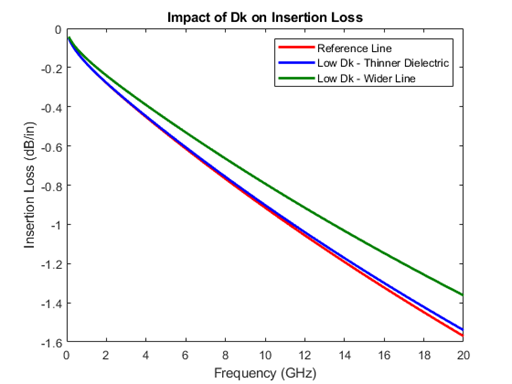
As can be clearly seen, the insertion Loss is almost the same for the Reference Line (with a 4.0 Dk) and the Low Dk–Thinner Dielectric line (with a 3.2 Dk). Essentially, whatever gain was offered from the Dk reduction was consumed entirely by the thickness reduction. However, there is a significant reduction in Insertion Loss from the Reference Line to the Low Dk–Wider Line (with a 3.2 Dk). For this reference example, a 20% reduction in Dk can result in either a reduction in thickness of 18.5%, a reduction in insertion loss of 13.2%, or some combination of the two (where the thickness is reduced by a certain amount less than the 18.5% possible, resulting in some reduction in insertion loss less than the 13.2% possible).
The Desirability of a Low DF Material Set
The argument for using a low DF material is simply that a lower dissipation factor results in lower dielectric loss (and, thus, lower insertion loss).
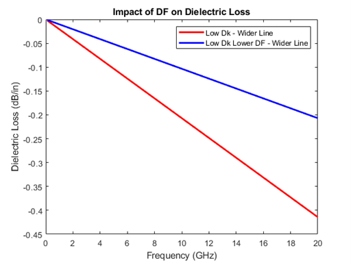
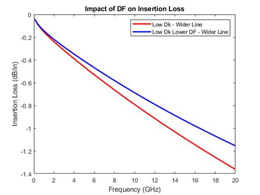
Let us explore another example, this time to illustrate the impact of DF on insertion loss. We start with the third stripline from Figure 1, built on a 3.2 Dk, 0.005 DF material, and then compare it with the same stripline structure built on a 3.2 Dk, 0.0025 DF material. Figure 2 shows the comparison between the dielectric loss values, while Figure 3 shows the comparison between the insertion loss values.
Manufacturing Tolerances
Such a treatment of these performance characteristics would be incomplete without at least mentioning the impact that manufacturing tolerances can have. Given that the dimensions of the copper traces, the dielectric materials, the dielectric properties, and roughness drive key performance measures such as impedance and loss, it becomes imperative to consider how tight or loose manufacturing tolerances can move a design from a pass to a fail. Figure 4 highlights this through an example of a differential stripline that is nominally ~85 Ω, but has a 95% confidence interval of ~78 Ω to ~91 Ω given the tolerances that are listed. This confidence interval is tightened significantly by reducing the tolerances in Figure 5, which shows a 95% confidence interval of ~81 Ω to ~88 Ω.
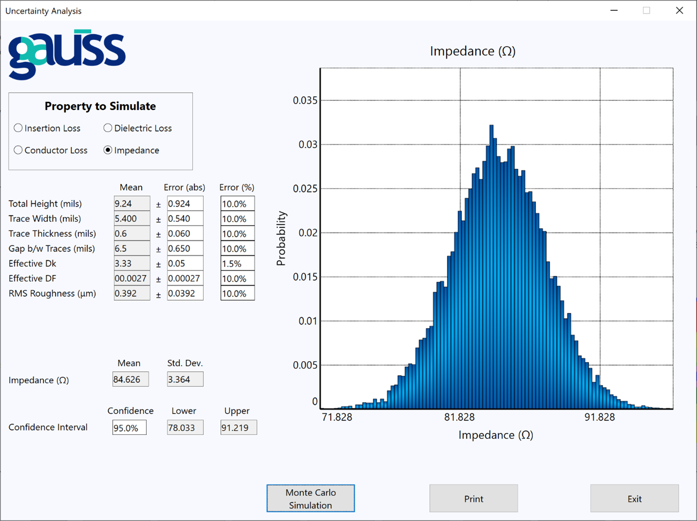 Figure 4. Uncertainty analysis for impedance with 10% geometric tolerance.
  Figure 5. Uncertainty analysis for impedance with 5% geometric tolerance.
 In reality, everything is stochastic. Small variations in key inputs can drive potentially significant variations in performance. Therefore, it is important to work back from what kind of variation in performance one can tolerate, which can then be used to determine what kind of variation one can tolerate within the inputs such that performance is kept within spec.
Summary
The most fundamental materials properties of relevance to the dielectric materials used in PCBs are the dielectric constant and the dissipation factor. They are central driving forces behind the two most critical Signal Integrity performance parameters: impedance and loss. It is important to go into the design and development process with a knowledge of what these key properties mean, how the materials vendors provide this data, as well as how tolerances and variations can impact performance. Visibility into these aspects is key to a successful product implementation.
Continue on to read Part 2 here.