
I hear board designers and engineers frequently mention current density while referring to or specifying designs. Current density can be defined as current per cross-sectional area. (DC) current is constant everywhere along a trace. But since area is a point concept, so then is current density a point concept. Current density comes up in several contexts. One is when referring to trace temperatures. A designer will ask about trace temperatures when given some assumed level of current density. I’ve heard engineers argue against using right-angle corners (one of my favorite topics) because the current density is highest going around the sharp corner and therefore will radiate most strongly at that point (wrong on several different levels!).
Spoiler alert
As a rule, I dislike giving away the punch line at the beginning of an article. But I think it is appropriate in this case. Current density can be an interesting concept. Graphics based on current density can be fascinating. But from a practical standpoint, current density is irrelevant. It is a consequence of other things, not a determinant of them. What follows will explain why.
Current density and trace temperature
Figure 1 represents a TRM (thermal risk management, Note 1) simulation model. The relevant parameters are (conversion to mils is approximate):
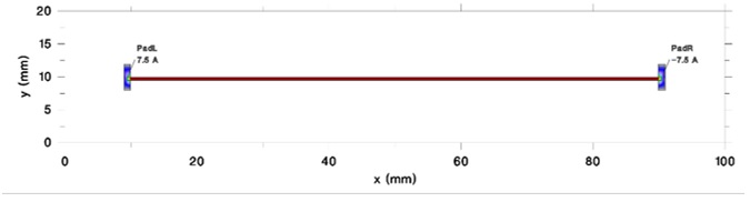
All trace combinations have identical cross-sectional areas, 0.075 mm2 (120 mil2). We applied 7.5 Amps through each trace combination and evaluated the current density and trace temperature. The results are shown in Table 1.

Current density and right-angle corners
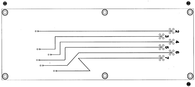
If you want to start a fight… find a room full of engineers, ask about right angle corners and EMI, and then shut the door. Or, go to the SI-List and ask the question.
The argument goes that current density is highest at the sharp bend of the corner (actually not true) and therefore EMI radiation will be highest at that point (also not true.) A landmark study was performed in 1998 that hoped to put this argument to bed (it didn’t!) (Note 3). Figure 2, from that study, illustrates a test board that was fabricated in order to measure radiated EMI from a variety of corner configurations. There were no significant differences in radiation from any of the traces, even the diabolically designed trace 7 with pointed 270 degree corners. Current density (and right angle corners) do not seem to be related to EMI.
Current (DC) follows the path of least resistance. The path of least resistance is the shortest path. The shortest path is right adjacent to the inside corner. So most of the current travels close to the inside corner, with some of it spreading out towards the outside corner.
As an aside, it should be noted that the cross-sectional area increases as we go around the corner. The trace thickness remains constant, but the width increases to its maximum (as much as 1.414 x W) at the middle of the turn. Therefore, the overall current density decreases in the corner area as we move towards the midpoint of the curve.
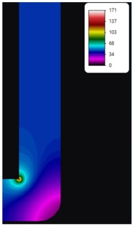
Figure 4 illustrates the thermal profile of the same simulation. Three points, A, B, and C, are shown in the figure. A and B are at the inside and outside edges of the curve in the trace. C is the midpoint of a straight section of the trace. The numbers beside the letters are the temperatures in oC at each respective point. Even though the current density (Figure 3) is much higher at point A in the model, the maximum temperature along the trace is at point C.
There are several dynamics at work here at the same time. First, the temperature is reduced in the curved area of the trace because the cross-sectional area of the trace is increased. The current is constant but the resistance decreases as the trace width increases. Therefore, the I2R heating component is reduced around the corner. Then, the inside edge of the trace is hotter because the cooling efficiency (of the board material) is much lower there than at the outside edge. The inside of the corner cools (conducts heat) into a 90-degree quadrant of the turn. Some of the straight portion of the trace also cools into this same quadrant. But the outside edge cools (conducts heat) into a 270-degree quadrant, that’s 300 % more area for cooling. The outside edge of the trace cools much more efficiently and therefore its temperature is much lower. None of this has anything to do with current density, which is a byproduct of the other things going on.

Current densities around vias
Figures 5 and 6 come from our via analyses. The details are not particularly import and can be found in our book (Note 4.) Graphics of current densities around vias are not particularly interesting. We showed in an earlier article (Note 5) that via temperatures are unrelated to current (or current density); they are determined by the trace temperature. So the current density patterns in Figure 5 are of only passing interest. At the risk of offending some engineers, however, I will comment that they do sort of resemble a hydraulic (water) analog of current flowing through a drain from one rectangular container to another!
Since the trace dimensions are perfectly symmetrical, so, too, are the current density patterns. Current density is highest at the leading edge of the top (front) layer and lowest at its trailing edge. Current density is highest on the bottom layer at the trailing edge. Not shown here is the current density pattern at the midpoint of the via. The current density is uniform around the circumference of the via at that point.
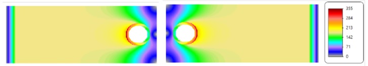
A more interesting situation is shown in Figure 6. A top trace is connected to a bottom trace, which is perpendicular to it, with four vias. The current between the trace segments divides between the four vias.
The current density is different around each via. That is because the shortest current path is through the inside via and the longest path is through the outside via. As mentioned above, simulations show that the current density in each via is uniform around its circumference at its midpoint. Knowing that current density, we can calculate the actual current through each via by multiplying the current density by the cross-sectional area of the via. As expected, the inside via carries the most current and the outside via carries the least. The other two vias share current equally. The sum of the currents in the four vias equals the applied current.
An unexpected result of our analyses is that if we measure the current “entering” each via by integrating the current density around the top of each via and multiplying by the via cross-sectional area, and then summing that all up, we get an answer greater than the applied current (a seemingly impossible answer.) The reason is that not all the current density at the top of the front vias represents current actually entering those particular vias. Some represents current “passing by” the front vias on the way to the back vias (Note 6).

Conclusion
While the current density patterns shown and measured herein are interesting, there is no practical relevance to them. They do not relate to trace temperature and they do not relate to EMI radiation. The measure of current density is a consequence of other relationships going on, not a determinant of them. Focusing on current density will not lead to any practical results.