
Return current for a signal always finds a way to flow as close to the signal as possible, thus minimizing the magnetic energy stored in the loop defined by the signal and its return path. So, the return current path is the combination of conduction paths that together minimize the stored magnetic energy. Some elements of the return current path may be part of the design and other elements may be unintentional.
In addition to the return planes and vias that are an important part of any printed circuit board (PCB) or package design, return current can transition directly between planes with little or no involvement from vias or other structures. The physical mechanism is magnetic coupling and the inductance introduced by this mechanism is closely approximated by the surprisingly simple equation
where µ0 is the magnetic permeability of vacuum (4π × 10−7 H/m) and d is the dielectric thickness between the planes. This approximation could be impaired if the plane transition occurs very close to the edge of the planar structure; however the effect is insignificant in most cases.
Consider, for example, the impedance inserted into a single-ended signal crossing a split plane. The most commonly expected return path is through a via to a decoupling capacitor and back through another via. Indeed, at frequencies for which the vias in this path are within a quarter wavelength of the signal trace, this conduction path can be an important component of the return current path. This is an area of ongoing study, and definitely needs to be confirmed through measured data.
However, our initial calculations suggest that the role of the return via may not be what is generally assumed. We are investigating the hypothesis that the primary role of the return via is to suppress resonances in a circuit board of finite size. In this context, a DC open circuit between planes is one such resonance. This hypothesis will be discussed in more detail in the Further Study section at the end of this article. The modeling and comparison to measured data in the next section does not include any effect due to return vias.
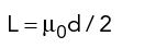
For a split plane crossing at higher frequencies, the conduction path through return vias is not significant because, by the time the return current flows out to the via and back on the other side, it arrives out of phase with respect to the signal current. Instead, as shown in Figure 1, the return current flows over the edge to the opposite face of the return plane. From there it couples to any plane that is adjacent to the return plane. In that plane it flows to the other side of the split, where the process is reversed. Each plane transition (down to the adjacent plane and back again) is essentially a half turn transformer whose inductance is L = µ0d/2, and the total impedance inserted by both plane transitions into the return path is Zsplit (ω) = 2 * jωL = jωµ0d.
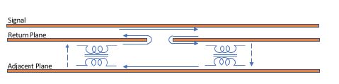
Figure 1. Split plane return current path.
This coupled path between planes can be both good and bad. When the plane adjacent to the return plane is relatively close, it can provide a low impedance return path at higher frequencies, which in most applications is good. However, if there is no adjacent plane at all, then the magnetic coupling is into free space, resulting in a transmitting antenna. That is bad in most applications. Also, if there is a lot of signal current crossing a split plane, as might be the case for a power distribution trace, then the return current will couple into traces in the adjacent routing layer. The designer should therefore be aware of the shape of the return current path.
Recognize also that in some designs, return current vias may not actually be carrying very much current, with most of the return current instead flowing by direct plane transition. It may be possible to remove some of those return current vias, saving board space and routing area. A disciplined engineering analysis should include direct plane transition in the equivalent circuits for critical interfaces.
This article compares this model to data measured to 30 GHz for the case of a widely used four contact PCB microwave probe site, and then presents a brief derivation of the equation given previously.
Demonstration and Validation
We will use a four-contact PCB probe launch site to compare the calculated equivalent circuit to measured data and to demonstrate how return current plane transitions occur for a structure that is more complex than a split plane transition. The geometry of the probe site is shown in Figure 2. The materials and geometries of the test board were chosen to be typical of a production design, with the possible exception that the stripline is more loosely coupled than is usual for high density routing. Note that the vertical scale is exaggerated to make it easier to visualize the return current paths.
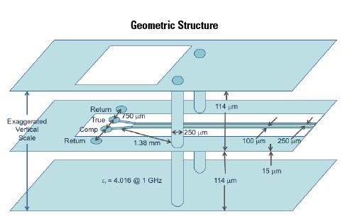
Figure 2. Four contact PCB probe site geometry.
The probe site enables microwave measurements of structures accessed by balanced transmission lines in either differential or single-ended mode. To create the probe site, the dielectric under the cutout on the surface of the board is removed to expose the contact points on an inner layer of the board. The inner contact points are for the true and complement signals, while the outer contact points are for the return current plane. While the probe site includes vias to connect the return current at lower frequencies, these vias were not included in the analysis presented here.
Because of the cutout on the surface of the board and the separation of the true and complement contact points, the two sides of the transmission line start out as uncoupled microstrip. The path then transitions to stripline at the edge of the cutout.
The return current paths for differential and single-ended modes are shown in Figure 3.
Figure 3. Differential and single-ended mode return current paths.
Where the probe contacts the PCB, the current in the return current contacts must find its way under the true and complement contacts. The return current vias are too far away to be of much help in the measurement frequency range, and so the return current transitions directly between planes as shown. There is a return path inductance between the return contact and the microstrip in the equivalent circuit provided in Figure 4.
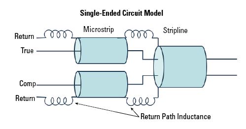
Figure 4. Probe launch equivalent circuit.
Figure 3 also illustrates the return current path at the edge of the top plane cutout, where the transmission line transitions from microstrip to stripline. In single-ended mode, half the return current must transition from the bottom return plane to the top return plane. The associated return path inductance between microstrip and stripline is also shown in Figure 4. However, in differential mode, the return currents on the two sides of the stripline have the same magnitude but opposite phase, and so cancel each other out at the transition from microstrip to stripline. This is also shown in Figure 3.
These probe sites were used on a test structure that was measured to 30 GHz using a vector network analyzer (VNA). Time domain reflectometry (TDR) traces were then computed from the frequency domain data, and the probe site was isolated at the beginning of each trace. For comparison, the element values in the differential mode equivalent circuit were computed directly from physical dimensions and materials properties, and a TDR trace prepared using the same methods as for the measured data. In the plots in Figure 5, the response of the two ends of the measurement test structure are shown in red, while the response of the equivalent circuit is shown in blue. It is readily seen that the model matches the measured data to within measurement error.
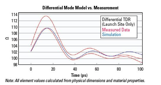
Figure 5. Model vs. measured data for differential mode.
As is usually the case, the data for single-ended mode was the data measured directly by the VNA, and the differential mode data was derived from that. We derived single-ended TDR traces for the probe sites from this data in the same way as for the differential mode data. The element values for the single-ended mode equivalent circuit above were calculated directly from physical dimensions and materials properties, and a TDR trace calculated for that circuit using the same methods as for the differential mode data. In the resulting plots in Figure 6, the TDR traces for the four single-ended ports are shown in red and the calculated response for the equivalent circuit is shown in blue.
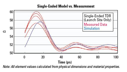
Figure 6. Model vs. measured data for single-ended mode.
Again, the model matches measured data within experimental error. It is interesting to note that even though the reference plane vias were closer to the microstrip to stripline transition than they were to the probe contact points, they were still not needed in the equivalent circuit.
Crosstalk
During the preparation of this article, a question was posed about the effect of return current plane transition impedance on the crosstalk between adjacent signals crossing the same plane transition. If the two signals are each single-ended, then each will encounter a plane transition inductance in its return path, and there will be some mutual coupling M between the two inductances. In general, 0 ≤ M ≤ 1, with the greatest crosstalk occurring for M = 1.
The electromagnetic analysis below could be extended to estimate the mutual coupling between two adjacent plane transitions. The basic procedure is to calculate the integral of the cross-product between the magnetic fields for the two transitions and divide by the integral of the product for a single transition with itself. Unfortunately, we do not currently have a closed form expression for this calculation.
We do, however, have measured data for the geometry and materials presented in Figure 2. As is typical for S-parameter measurements using a VNA, the data included measurements of single-ended crosstalk between the two traces that make up the differential transmission line. Voltage waveforms were calculated both for the single ended TDR and the time domain transmission (TDT) waveform for the adjacent trace, and these waveforms are shown in Figures 7 and 8, respectively.
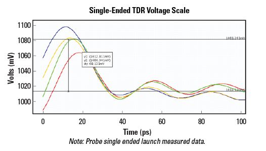
Figure 7. Single-ended TDR voltage waveform for probe launch.
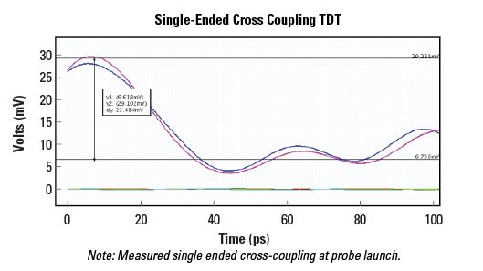
Figure 8. Single-ended cross-coupled TDT waveform for probe launch.
The amplitude of the inductive bump at the beginning of the cross-coupled TDT waveform is approximately three tenths of the amplitude of the inductive bump at the beginning of the TDR waveform. So the mutual coupling is M ≈ 0.3. While the trace spacing for the geometry measured is relatively loose for differential routing, it is about as tight as spacing typically gets for single-ended routing. This single data point, then, should provide some useful guidance on the crosstalk to be expected at a plane transition.
Electromagnetic Analysis
The electromagnetic analysis assumes that the relevant eigenmode is a first-order radial transverse electromagnetic (TEM) wave.1 That is, a wave with electric field perpendicular to the planes propagates radially from the point where the return current crosses the edge of the plane. The amplitude of the wave varies from zero in the direction of the plane edge to a maximum in a direction perpendicular to the plane edge.
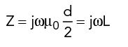
The analysis further assumes that the center of the radial TEM wave is at some small distance r from the plane edge, and that the return current flows inside the contour shown in Figure 9. The contour extends to infinity at the top and bottom, and it is inside the return plane on the left hand side of the contour. The analysis is completed in closed form, producing an impedance in terms of Bessel functions. The Bessel functions were replaced by their approximations for small arguments. In that form, the limit as r approaches zero produces the plane transition impedance given at the beginning of this article.
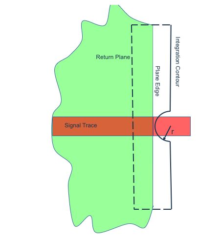
Figure 9. Integration contour for magnetic field.
Following the formulation1, and using the Hankel form of the Bessel functions, the fields in this case are
where k is the propagation constant (wavelength divided by 2π) and η is the propagation impedance of the dielectric. Since almost all PCB and package dielectrics have the same magnetic permeability as free space, the remainder of this derivation will use µ = µ0, in which case
The wave propagates in the direction ϕ = π/2 and so the voltage in that direction is simply
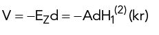
The current is calculated by integrating the magnetic field around the integration contour. Since the left hand half of the integration contour is inside the reference plane conductor, the contribution from that portion of the contour is zero. Also, since the radial magnetic field Hr is symmetric with respect to the integration contour, the contribution from that component of the magnetic field drops out as well. The only remaining term is the integral of the tangential magnetic field Hϕ around the semicircular arc in the center of the contour. This yields
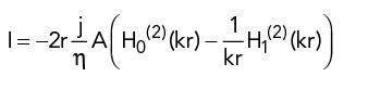
The resulting impedance is
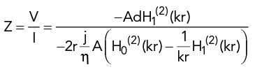
Taking the limit as r approaches zero produces
Further Study: The Role of the Return Via
Our initial estimate of the effect of the via path assumed that the planes were infinite or semi-infinite. In this model, the via path is only significant when the distance between the return via and the signal trace plane crossing is comparable to the separation between return planes.
Our initial analysis did not, however, consider the effect of finite plane size. Parallel planes of finite size can support many resonant modes, especially if the planes are not connected directly together. For example2, we measured the response of a pair of parallel circular planes with and without return vias connecting them. The results are shown in Figure 10 and have since been matched by analysis using closed form equations.
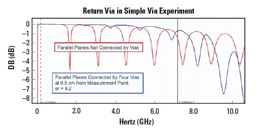
Figure 10. Measured insertion loss of disk without and with return vias.
Figure 10 also shows the frequency at which the return vias are one quarter wavelength from the measurement point. In this data, the return vias were almost completely effective in suppressing the resonances below the quarter wavelength frequency and not at all effective in suppressing resonances above that frequency.
The structure and propagation mode associated with Figure 10 are different from the structure and propagation mode associated with return current plane transition. Nonetheless the same principle may apply. In other words, the return current plane transition may behave as though the planes are infinite below the return via quarter wave frequency but then be disrupted by plane resonances above that frequency. For example, it may be that a resonant mode applies much larger fields to a return via, magnifying the effect of the return via on the overall response.
It is important to continue to study the specific behavior of return vias because they tend to consume much-needed routing space. Return vias should therefore be placed where they are going to be most effective.n
References
1. S. Ramo, J. R. Whinnery, and T. Van Duzer, “Fields and Waves in Communications Electronics, Third Edition,” John Wiley and Sons Inc., Section 9.4, 1994, pp. 468–470.
2. C. Ding, D. Gopinath, S. Scearce, M. Steinberger, and D. White, “A Simple Via Experiment,” DesignCon, February 2009.
Article was published in the SIJ January 2020 Print Issue, Technical Feature: Page 30.