
The goal of power integrity (PI) analysis is to ensure not only sufficient but also stable power to all chips in a system. With ever increasing printed circuit board complexity and decreasing system size, ensuring that critical chips receive stable power is becoming more important. Optimizing their location and value as early as possible in the design phase will reduce the risk of late stage design changes or board re-spins. Stability of the power rail to critical chips can be ensured by keeping the impedance of the power rail below a specific target [1].
Decoupling capacitors are an inexpensive method of lowering impedance over a range of frequencies. There are many possible parameters to sweep and consider when selecting on-board decoupling capacitors to optimize power plane impedance [2]. Not only can we consider the number of capacitors and their placement, but we should also sweep their capacitance, equivalent series inductance (ESL), equivalent series resistance (ESR), and their mounting inductance in reducing the power plane impedance below a safe target.
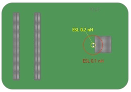
Many of the parameters in this long list can be simplified into a single measure called the “effective radius” of a capacitor [3]. The effective radius tells us the approximate distance around a capacitor where it is effective at reducing power rail variations. The effective radius varies with frequency and is reduced significantly with increased ESL (Figure 1).
Layout changes of the power rail can cause large variations in the loop inductance contribution of each on-board decoupling capacitor. Reducing the loop inductance seen from the power pins of chips to the capacitors is a key metric in determining which decoupling capacitors will be most effective in reducing power rail impedance. Furthermore, optimizing decoupling capacitor placement using loop inductance is a no-cost method of lowering your rail’s impedance and increasing your power delivery network (PDN) stability.
Here we show a quick optimization process for decoupling capacitor placement and selection in a DDR-4 design consisting of a memory controller with two daisy chained dual in-line memory modules (DIMMs). The design is in the post-layout stage where the need for quick analysis and feedback to the layout designers is key. We analyze the impact of decoupling capacitor changes using a hybrid solver with an adaptive finite element mesh in two dimensions. We focus our analysis below 20 MHz, where the impedance of surface mount capacitor components used in PCB designs can have a big impact.
At these frequencies, the wavelength of electromagnetic energy is 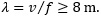 . The wavelength is calculated from the speed of the electromagnetic energy,
  where c is the speed of light in air, and we assume a relative dielectric constant,
  , common for FR-4 based designs. Since the wavelength is significantly greater than the size of the PCB design we are considering, the quasi-static approximation holds, and our simulations can provide quick feedback to the board design team.
Figure 2 shows a cross-sectional view of a PCB with a single power rail feeding a chip. The many types of decoupling capacitors that can impact your power rail are shown, including bulk decoupling capacitors near the VRM, surface mount capacitors near the chip, and on-chip capacitors embedded inside the package. These different capacitor types contribute to lowering the power rail impedance over different frequency ranges. Here we will focus on the placement of surface mount capacitors near the IC since board design teams often have considerable flexibility in their placement and selection.
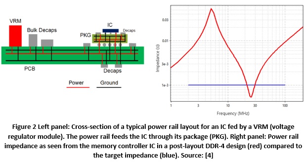
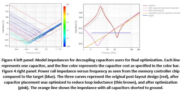
Looking at the impedance of the power rail from our DDR-4 memory controller chip, we see that it is exceeding the target impedance at many frequencies (Figure 2 right panel). This design has already been laid out and is using over 100 decoupling capacitors on this power rail, but our impedance is still exceeding the target by more than 10x at some frequencies. Target impedances are set to keep noise margins on the power rails in a safe range. When the power rail impedance exceeds the target significantly, any transient power current noise can lead to dangerous levels of voltage noise for any chips connected to the rail. Improving our power rail impedance on this DDR-4 design will greatly reduce the risk that we will require a design re-spin due to noise on the memory controller chip.
We first consider the placement of the decoupling capacitors on the board by simulating their loop inductance to the pins of our chip. To perform this analysis, our hybrid simulator creates a measurement port at the power pins of the chip and shorts the capacitor terminals to give users the loop inductance due to the PCB layout alone. From this analysis, we found four decoupling capacitors on this power rail far away from our chip. There is space on our board to move two of them closer. This simple change decreases the impedance seen from our rail getting us closer to the target impedance at no additional fabrication cost (Figure 4).
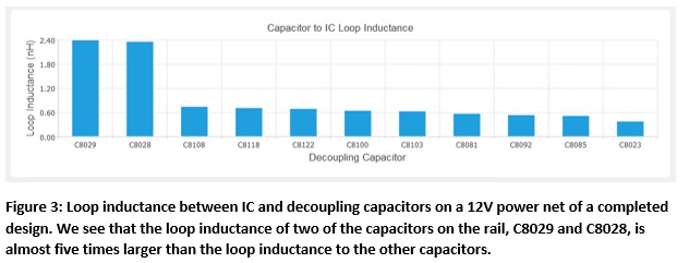
We performed a chip to decoupling capacitor loop inductance analysis of 10 completed designs. In more than half of these designs we found ineffective capacitor placement as measured by the loop inductance on the power plane. For example, looking at the loop inductance between one component to all the decoupling capacitors on the 12V rail of a completed design, we see that two of these capacitors have loop inductances that are five times larger than the other capacitors on this rail (Figure 3).
The placement of these capacitors makes them ineffective, and the high loop inductance of the rail to these devices makes them more prone to generate or pick up noise on the very dense PCB design. This means that their presence on the board provides little benefit and can actually cause harm to sensitive signal nets nearby.
Coming back to our DDR-4 post-layout design, we next consider an optimization looking at the number and type of capacitors in the design. The left panel of Figure 4 shows the different capacitor models used in the optimization process. Our optimization takes less than 30 minutes to analyze more than 100 decoupling capacitors placed in this design, and we achieve a result that is below the target up to 10 MHz. We see that even with all capacitors shorted to ground, the impedance of the power rail above 10 MHz increases above the target impedance (Figure 4 right panel).
The final scheme includes the same number of capacitors as the original design but can achieve significantly lower power rail impedance. Although a complete analysis of the PDN should also include the bulk capacitors connected to the VRM and the on-package decoupling capacitors, their impact will be greatest at lower and higher frequencies, respectively. Here we show the frequency range most relevant to on-board surface mount capacitors.
[1] Smith, L. D. and Bogatin, E. Principles of Power Integrity for PDN Design Simplified. Prentice Hall, 2017. pp 10-12.
[2] Novak, I. “Comparison of Power Distribution Network Design Methods: Bypass Capacitor Selection Based on Time Domain and Frequency Domain Performances.” TecForum MP3, DesignCon 2006.
[3] Chen, Huabo, Jiayuan Fang, and Weimin Shi. "Effective decoupling radius of decoupling capacitor." IEEE 10th Topical Meeting on Electrical Performance of Electronic Packaging. IEEE, 2001.
[4] Team-based PDN Design with PowerTree, PowerDC, and OptimizePI Rapid Adoption Kit. http://support.cadence.com 2017.