
Analysis of Data
Two interesting outliers are observed in Figure 8. Device F contains an outlier for the combined PN + S/A methods, and Device H contains an outlier for the phase-noise-with-flat-extension methods. Alternatively, device G produced somewhat matching results for all methods. Figure 9 (a) isolates these three devices for a few interesting methodologies, and maps them to their smoothed spectrums in Figure 9 (b) for further analysis.
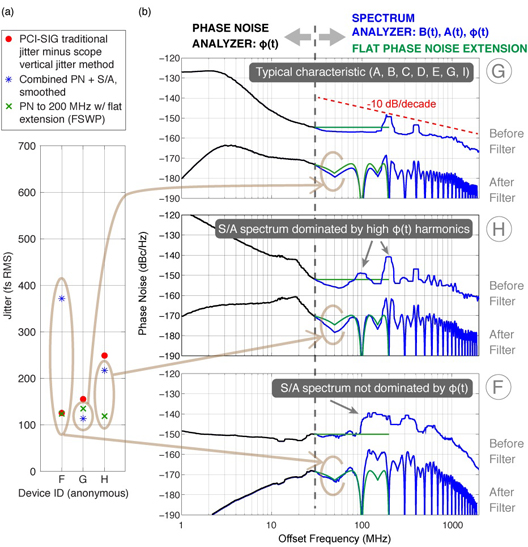
Figure 9. Detailed analysis of outlier data from devices F and H, compared with reference device G
The methods shown in Figure 9 (a) for device G match jitter relatively well, as they do for devices A-D, E and I. Interestingly, the spectrums shown in Figure 9 (b) for device G show the flat-extension region overestimates the observed phase noise, which rolls off with increasing offset frequency. On the other hand, the flat-extension region ends at 200 MHz, which underestimates the observed phase noise compared to the oscilloscope method that aliases phase noise up to at least its 2 GHz acquisition bandwidth. This data suggests that the error introduced by these two non-idealities cancel each other out at an optimum upper-integration limit of 200 MHz.
The author speculates that the reason why this 200 MHz offset frequency leads to an accurate estimate of jitter is because the amplitudes of harmonics (in an ideal square wave) decrease with increasing frequency [14], such that the 3rd harmonic of a 100 MHz digital clock signal, which occurs at a 200 MHz offset frequency, is larger than all higher harmonics. Therefore, the 3rd harmonic's contribution to jitter can be larger than the contribution from higher harmonics.
If we assume the spectrum analyzer data for device G in Figure 9 (b) represents phase noise, then the region that dominates the integral of the spectrum analyzer's phase noise can be located by drawing a -10 dB/decade line above the curve, and lowering it until it intersects the curve [15]. The point of intersection identifies the dominant contribution to this integral, or jitter value. This intersection is observed to occur at the 3rd harmonic for device G in Figure 9 (b). The phase noise spectrum rolls off significantly above the 3rd harmonic and can be safely ignored. The dominant contribution to jitter can thus be captured by integrating to an offset frequency equal to twice the clock frequency (i.e. the 3rd harmonic).
By extending the last-measured phase noise data point to twice the clock frequency as shown by device G in Figure 9 (b), the green curve representing the phase noise extension overestimates phase noise between 30 and 150 MHz offsets, and underestimates phase noise between 150 and 200 MHz offsets, compared to the blue curve representing spectrum analyzer data (note, integrating a logarithm x-axis gives more weight to areas at higher frequencies). These opposing factors cancel out, causing the integration of the filtered phase noise with flat extension to 200 MHz to approximate the true jitter.
Let's next analyze the outlier for device F in Figure 9 (b), which shows a large increase in spectral energy density starting at 100 MHz offset. Since spectrum analyzers measure both amplitude noise/modulation and phase noise, this increase seems to be caused by something other than phase noise, particularly considering the excellent match that the integrated phase-noise-with-flat-extension method provides to the oscilloscope-derived jitter in Figure 9 (a). The device F spectrum analyzer data therefore overestimates the contribution of jitter due to phase noise when integrated. Unfortunately, phase noise data derived from spectrum analyzers always have this potential issue. While phase noise analyzer instruments can also separately measure amplitude modulation, this capability does not extend beyond a few tens of MHz in offset frequency. Thus, there does not appear to be an easy way to screen for when amplitude noise/modulation dominates in a spectrum analyzer plot of phase noise.
It is also interesting to note that the frequency spacing between data points located near spectral boundaries defined at integer multiples of the Nyquist frequency (e.g. 50 MHz, 100 MHz, 150 MHz, etc.) using the spectrum analyzer are spaced much too far apart to follow the filter curvature at these boundaries as shown in Figure 4 (b). That is, the frequency spacing between phase noise data at 200 MHz offset obtained with a spectrum analyzer is on the order of MHz, whereas filter changes near the 200 MHz offset occur in the kHz scale. This introduces another potential source of large error for spectrum-analyzer based methods. For these reasons, we hesitate to recommend a jitter methodology derived from spectrum analyzer data [8].
Device H presents a second outlier. Here, the phase-noise-with-flat-extension method shows a poor match. Analyzing device H in Figure 9 (b), large harmonics are observed. The second harmonic (200 MHz) occurs at an offset (from the 100 MHz carrier) frequency of 100 MHz; the third harmonic (300 MHz) occurs at an offset frequency of 200 MHz, and so on. These harmonics are captured by spectrum analyzer and oscilloscope based methods, but not by the phase-noise-with-flat-extension method (causing it to underestimate the real jitter). A device with large harmonics has a very high and broad phase noise skirt, or near-in phase noise, at its fundamental (100 MHz) clock frequency. Such a device is typically not intended for jitter-critical applications. For example, PCI Express 5.0 [5] limits refclk jitter to 150 fs RMS.
Figure 10 illustrates how such devices can be easily screened via a phase noise mask test, with spurs omitted. For example, devices H and I fail the mask test due to their high near-in phase noise. The rest of the devices pass the mask test, and can be subsequently filtered and analyzed as above. This approach is similar to an eye-mask test common in many high-speed serial-data communication standards, in that passing the eye mask test is a necessary but not sufficient condition to proving jitter compliance (a more detailed bathtub or other jitter compliance test is subsequently required).
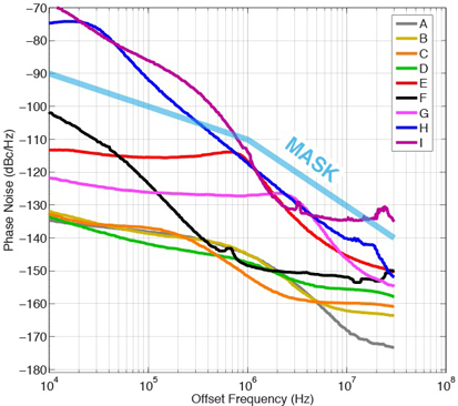
Figure 10. To improve matching, a phase-noise mask test can screen out clock devices having unrealistically high near-in phase noise
The Recommended Phase-Noise Methodology
From Figure 8, the phase-noise based methodology that provided the best match to jitter from the oscilloscope-based methodology is the phase-noise-to-200-MHz-flat-extension method [7]. To eliminate additional jitter added by the oscilloscope, phase noise introduced by the oscilloscope's time base can be integrated and subtracted from the oscilloscope jitter results. Unfortunately, we don't have access to, and therefore cannot measure, the oscilloscope's internal time base phase noise. We can, however, estimate the oscilloscope's time base jitter from Figure 8 by first assuming that the lowest value of jitter measured for the phase-noise-to-200-MHz-flat-extension method, which occurs for device A (and is 27 fs RMS), provides a "true" value of jitter.
Then, assuming random components of jitter dominate, we can perform quadrature subtraction of this jitter value from the filled-red "o" values (i.e. PCI-SIG traditional jitter method minus scope vertical jitter) shown in Figure 8. These new values are plotted using filled-orange "o" symbols in Figure 11, and labeled in the legend as the "PCI-SIG traditional jitter method minus scope vertical and horizontal jitter." Additionally, Figure 11 plots E5052B test results for the phase-noise-to-200-MHz-flat-extension method using green "−" symbols, which agree well with FSWP data obtained using the same method.
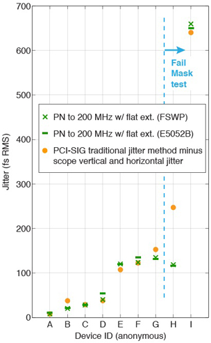
Figure 11. The final phase-noise based methodology produces jitter values matching those from the traditional oscilloscope-based methodology after subtracting jitter introduced by the measurement environment
In summary, Figure 11 shows excellent agreement between the traditional PCI-SIG oscilloscope-based jitter methodology (with environment jitter removed) compared with a new phase-noise based methodology based on extending the last-measured phase noise data point to 200 MHz (the phase-noise-to-200-MHz-flat-extension method). The procedure may be summarized for PCI Express as follows, with reference to Figure 12.
- Measure a DUT's raw phase noise in dBc/Hz using a phase noise analyzer.
- If spread-spectrum clocking (SSC) is enabled, remove SSC spurs below 2 MHz as required by PCI-SIG.
- Omit all spurs from the phase noise spectrum and evaluate it against a predetermined phase noise mask (an example mask is shown in Figure 12). If the DUT passes, continue to the next step.
- Extend the phase noise plot from step 2 with a straight line up to twice the clock frequency (i.e. 200 MHz offset frequency, equivalent to the 3rd harmonic, or 300 MHz, in the signal spectrum).
- Mirror the jitter filter across spectral boundaries located at integer multiples of the Nyquist frequency (e.g. 50 MHz), up to twice the fundamental clock frequency (i.e. 200 MHz offset frequency). Alternatively (not shown), alias phase-noise data (from step 4) located above the Nyquist frequency to below the Nyquist frequency.
- Filter the phase noise data.
- Derive an RMS jitter value by integrating the filtered phase noise data, as illustrated by the shaded area labeled "Integration Region" in Figure 12.
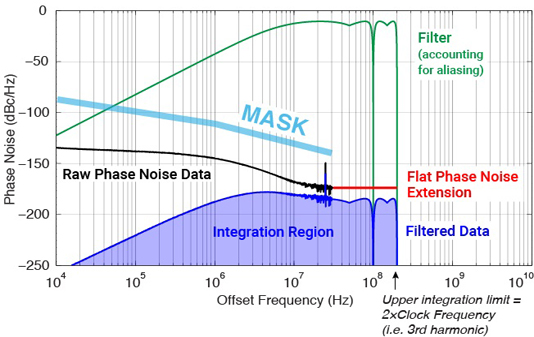
Figure 12. Summary of the recommended phase noise methodology, which appends a flat phase-noise extension up to twice the clock frequency, before filtering and integrating to derive jitter [7]
PCI-SIG adopted this procedure (without step 3) in PCI Express Base Specification Revision 5.0 Version 0.9 [16]. Note that certain aspects of the filtering process are patent pending [7].
Conclusion
The clock and timing industry typically derives jitter in clock signals from phase noise analyzer measurements. On the other hand, high-speed serial-data communications standards typically measure jitter in serial-data signals using an oscilloscope. PCI Express is one of the few standards specifying reference clock jitter requirements. Historically, PCI-SIG required refclk jitter to be measured using a real-time oscilloscope. Recent increases in data rates require lower-jitter reference clocks, to the point where today, jitter added by an oscilloscope-based test environment can no longer be ignored. This motivated creating a methodology based on phase noise that yields the same jitter values obtained via the traditional PCI-SIG oscilloscope methodology. To find a suitable methodology, this article analyzed nine clock devices from four manufacturers using various oscilloscope and phase noise methodologies.
The results show that the traditional method of extending and integrating phase noise up to the Nyquist frequency ignores aliasing and thus underestimates jitter compared to that observed by an oscilloscope or real system. By understanding how phase noise aliases in sampled systems, we created a methodology to filter phase noise and derive jitter [7]. Empirically, we refined this method to post-process phase noise by extending the last-measured data point up to an offset frequency equal to twice the fundamental clock frequency. The final recommended phase noise methodology produced jitter values matching those from traditional oscilloscope-based measurements after subtracting jitter added by the oscilloscope. As a result, this phase-noise methodology was adopted into PCI Express Base Specification Revision 5.0 Version 0.9 [16] as an alternative normative test to the traditional PCI-SIG oscilloscope-based refclk jitter methodology.
Incidentally, the data-converter industry empirically derived (at least a decade earlier) the same phase-noise upper-integration limit of twice the fundamental clock frequency, based on signal-to-noise measurements on data converters [17-19]. This article provides an independent analysis justifying this "2x" rule of thumb.
Note that, in keeping with PCI-SIG requirements, spurious phase noise (other than from SSC) is assumed small and therefore not omitted during post processing. However, other standards wishing to adopt this methodology may choose to omit spurs when deriving an random component of jitter. Although the above discussion addresses mainly random phase noise to obtain a random (RMS) component of jitter, a similar analysis can be made for the spurious phase noise spectrum to derive a deterministic (peak-peak) component of jitter value.
In summary, the phase noise methodology presented here is much faster and simpler to implement than the corresponding oscilloscope methodology. Since a phase noise analyzer has a lower noise floor than an oscilloscope, this methodology also scales more easily as timing margins shrink in future high-speed serial links. Finally, this methodology is a more natural fit for analyzing clock signals than an oscilloscope methodology, since phase noise data is readily available for precision clock sources.
Article was published in the SIJ July 2019 Print Issue, Technical Feature: Page 42.
Disclaimer
PCI, PCI Express, PCIe, and PCI-SIG are trademarks or registered trademarks of PCI-SIG. All opinion, judgments, and recommendations presented herein are the opinions of the author and do not necessarily reflect on the opinions of the PCI-SIG.
References
[1] "PCI Express Base Specification Revision 4.0 Version 1.0," PCI-SIG (Sept. 27, 2017), www.pcisig.com
[2] "NOTE-5, Removing Oscilloscope Noise from RMS Jitter Measurements," G. Giust, F. Benford, Technical Note, JitterLabs (July 25, 2017), https://www.jitterlabs.com/support/publications
[3] "Refclk Fanout Best Practices for 8GT/s and 16GT/s Systems," G. Richmond, SiLabs, PCI-SIG Developers Conference in Santa Clara, CA (June 7, 2017), www.pcisig.com
[4] "PCI Express Measurement Techniques for Gen5 and Beyond White Paper," R. Wade, J. Hsu, J. Tajnai, J. Bal, IDT (Jan. 9, 2018), https://www.idt.com/document/whp/pcie-measurement-techniques-gen5-and-beyond-white-paper
[5] "PCI Express Base Specification Revision 5.0 Version 0.9," PCI-SIG (Oct. 18, 2018), www.pcisig.com
[6] "Phase Noise Aliases as TIE Jitter," G. Giust, Signal Integrity Journal (July 23, 2018), https://www.signalintegrityjournal.com/articles/912-phase-noise-aliases-as-tie-jitter
[7] "Method and Apparatus for Analyzing Phase Noise in a Signal From an Electronic Device", patent pending, JitterLabs LLC, www.jitterlabs.com
[8] "Influence of Noise Processes on Jitter and Phase Noise Measurements," G. Giust, Signal Integrity Journal (April 8, 2018), https://www.signalintegrityjournal.com/articles/800-influence-of-noise-processes-on-jitter-and-phase-noise-measurements
[9] "Methodologies for PCIe5 Refclk Jitter Analysis," G. Giust, PCI-SIG Electrical Workgroup Meeting (Jan. 19, 2018), www.pcisig.com
[10] "Study to Determine a Phase-noise Methodology that Matches Jitter Measurements from a Scope," G. Giust, rev. 6, PCI-SIG Electrical Workgroup Meeting (May 24, 2018), www.pcisig.com
[11] "NOTE-3, How to Setup a Real-time Oscilloscope to Measure Jitter," G. Giust, Technical Note, JitterLabs (Feb. 16, 2016), https://www.jitterlabs.com/support/publications/note3/note3
[12] "Measuring Phase Noise with Baluns," G. Giust, D. Jorgesen, Microwave Journal, vol. 59, ed. 10 (October 2016), pp. 84-100.
[13] "Characterizing a Signal in the Presence of Noise", patent pending, JitterLabs LLC, www.jitterlabs.com
[14] "Signal and Power Integrity - Simplified (3rd Edition)," E. Bogatin, Prentice Hall (Jan. 12, 2018), Chapter 2.7.
[15] "Determine the Dominant Source of Phase Noise, by Inspection," G. Giust, Note-4, JitterLabs LLC, https://www.jitterlabs.com/support/publications/note4/note4
[16] "PCI Express Base Specification Revision 5.0 Version 0.9," section 8.6.7, PCI-SIG (Oct. 18, 2018), www.pcisig.com
[17] "Sampled Systems and the Effects of Clock Phase Noise and Jitter," B. Brannon, AN-756, Analog Devices (2004), www.analog.com/AN-756
[18] "Analog-to-Digital Converter Clock Optimization, A Test Engineering Perspective," R. Reeder, W. Green, R. Shillito, Analog Dialogue, 42-02, Analog Devices (Feb. 2008), https://www.analog.com/en/analog-dialogue/articles/analog-to-digital-converter-clock-optimization.html
[19] "Interfacing to Data Converters," W. Kester, Analog-Digital Conversion, Chapter 6.5, Analog Devices, https://www.analog.com/media/en/training-seminars/design-handbooks/Data-Conversion-Handbook/Chapter6.pdf