
That’s the question that will trigger your amygdala’s fight or flight response as you encounter the many annoyances that PAM4 brings to your world. Since you’re in a lab rather than a jungle, that fight or flight response might translate into sarcastic cracks like: “Right, that higher BER requirement makes it all so much easier—not.” “Good old NRZ, those were some fine bits. Remind me why I asked for this?” And, “dear NRZ, I never knew how much I loved you until I lost you.”
Four-level pulse amplitude modulation, PAM4, is being implemented in many 25+ Gb/s signaling schemes and most 50+ Gb/s standards. All the problems that PAM4 “solves” can be traced back to the channel response at high frequency. Insertion and return loss increase exponentially with frequency in PCB (printed circuit board) which causes two big problems. First, attenuation of peak-to-peak voltage swings to a tens of mV or less, and, second, massive signal degradation due to ISI (inter-symbol interference) that’s beyond the help of equalization. Add to these two design nightmares that smaller UIs (unit intervals) mean faster rise and fall times which enrage crosstalk aggressors, and you get a signal integrity nightmare that calls for radical action: PAM4. But don’t celebrate. While PAM4 addresses all of these problems, it solves none of them.
PAM4 is summarized in Figure 1. Where NRZ (nonreturn to zero) modulation encodes one bit per UI (unit interval), logic 0s at low amplitude and logic 1s at high amplitude, PAM4 encodes two bits in each of four levels. Each level, whether a voltage level or optical power level (don’t forget the factor of two when you convert voltages to decibels!), is referred to as a “symbol.” Like in the olden days of dial-up modems, we have to distinguish bit/rate from baud: two bits per symbol means that the PAM4 bit rate is twice its baud, e.g., 100 Gb/s PAM4 operates at 50 Gbaud.
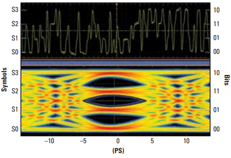
Figure. 1 The PAM4 signaling scheme (graphic Copyright Tektronix, used with permission).
Notice that we can assign pairs of bits to each of the four levels however we want; this is called Gray coding after Frank Gray who patented this sort of thing in 1947. The coding scheme shown in Figure 1, with 11 assigned to the third highest level (S2), and 10 assigned to the highest level (S3), decreases the probability of a symbol error causing two bit errors; which also helps the SER (symbol error ratio) converge to the BER (bit error ratio), which is nice.
For a given data rate, PAM4 operates at half the bandwidth of NRZ, and that’s where its advantages end. The costs of that factor of two in bandwidth include (see Table 1) three eye diagrams in each UI, 9.5+ dB drop inSNR (signal-to-noise ratio) for electrical and 4.7+ dB for optical signals (see? I told you not to forget that voltageto-power factor of two),12 separate logic transitions, 6 distinct rise and fall times, 75% transition density, potential for misalignment of those three eye diagrams in both voltage (or power) and time, and a minefield of mixed blessings involving how these problems are addressed.

Table 1. Regretting the PAM4 decision and reminiscing about the good old days with NRZ.
Okay, it sounds pretty grim, but if you’ve been looking for a chance to exercise your innovative prowess, in a few minutes you’ll see that PAM4 makes a fine playground.
Since intersymbol interference (ISI) and crosstalk are both types of amplitude noise, PAM4’s SNR drop is a big deal. Each of the three PAM4 eye diagrams suffers, and we have to do something drastic: use FEC (forward error correction). You can think of FEC as CRC (cyclic redundancy check) on steroids. The high-speed serial standards use Reed Solomon FEC schemes. RS-FEC introduces overhead bits to the data, usually just a few percent overhead can reduce the BER by more than a factor of a million. RS-FEC uses a shift register based on special binary polynomials at the transmitter to encode the data and overhead bits and then inverts the process at the receiver. The decoding process automatically corrects a limited number of errors—if you ever get a chance to step through FEC software line-by-line, go for it, watching the algorithm flip errored bits is as close to pulling rabbits out of hats as I’ve ever seen in a debugger—but it costs power, latency, and silicon real estate at both the transmitter and receiver.
For example, 400 Gigabit Ethernet uses RS-FEC(544, 514) which is capable of correcting at least 15 and as many as 150 errors in every sequence of 5440 bits. The number of errors it can correct depends on the locations of the errors in the 5440 bit sequence. Not bad, worst case you can fix a BER of 15/5440 = 2.7E-3, which is almost a billion times the 1E-12 BER that your design probably needs to meet.
You turn to your oscilloscope, mutter, “Problem solved,” and head for the coffee station—but not so fast!
Yes, with FEC the BER requirement is relaxed from 1E-12 way up to 1E-6, 1E-5, or even 1E-4 depending on the standard, but there’s a catch. Compared to the tight ship we sailed with NRZ, which in most cases ran pretty much error free, we’re now so relaxed that we anticipate pre-FEC errors on the scale of one in a million. “But it’s cool,” you say, slurping the whipped cream off your Frappuccino, “FEC will fix it, game over.”
While PAM4 has relieved us of a factor of two in bandwidth, its reduced SNR makes it more vulnerable to amplitude degradations of all types, including ISI and crosstalk. It’s not crippling, as it would be with NRZ, but it won’t be easy either. We still have to equalize ISI in every way can. The approach we’ve used for NRZ includes FFE (feed-forward equalization) at the transmitter and either or both CTLE (continuous time linear equalization) and DFE (decision feedback equalization) at the receiver: see Figure 2. This robust equalization scheme runs into problems when combined with error correction.

Figure 2. Typical high speed serial receiver architecture for NRZ signals with a two tap DFE (graphic copyright Ransom’s Notes, used with permission).
Remember, DFE operates on the assumption of a low BER: Logic decisions are fed back, added to the output of the CTLE, and the resulting signal is sent to the logic decoder, a.k.a., slicer. When DFEs feed back errors, they deteriorate the signal at the slicer which can cause another error and the problem gets worse. The result is the well known tendency for DFEs to cause burst errors when they fail. Data scrambling and interleaving can stir the burst errors into multiple RS-FEC blocks, which helps, but RS-FEC usually can’t accommodate both the high pre-FEC BER and DFE-caused burst errors.
When the errors are either too numerous or in an unfortunate order or both, FEC can’t correct any of them and we’re left with a system operating at a BER of 1E-7 or higher—total failure! Back in the good old days with NRZ, when we had a few errors, the BER might degrade to 1E-11, maybe even 1E-10, but NRZ systems that operated at BERs around 1E-7 or higher were intolerable. They’re no less tolerable for PAM4 systems.
The solution is to give up on DFE. Yes, it’s drastic; a total revision of receiver design and the need for a new equalization scheme.
The minimal design readjustment is to combine FFE at the transmitter with a more flexible CTLE at the receiver, Figure 3: three poles and gain adjustable in halfdB steps instead of the two poles and 1 dB gain steps that we use for NRZ.

Figure 3. More flexible CTLE for PAM4.
Since CTLE alone wasn’t always sufficient for NRZ, we don’t really expect it to suffice for PAM4. The next improvement is to add FFE at the receiver. Mathematically, receiver FFE is the same as transmitter FFE,
FORMULA
where Rx(n) and e(n) are the received and equalized levels of the nth bit, respectively, and ki are the equalization correction constants, a.k.a., taps.
The design difference is huge, Figure 4: where DFE operated with discrete logic levels from the slicer output, receiver FFE applies taps to symbol voltage levels. In other words, receiver FFE requires an ADC (analog to digital converter) in the receiver. Implementation of an ADC requires more power and silicon space.
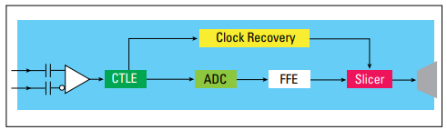
Figure 4. Receiver architecture with FFE instead of DFE.
Here’s where it gets interesting. Once you’ve paid the price for an ADC, why stop there? Once you’re playing with symbol voltage levels, a whole world of signal optimization algorithms opens up. If you have to put in an ADC, why not install a DSP (digital signal processor) and let your imagination run wild, Figure 5?

Figure 5. DSP-based receiver architecture.
DSP allows for the whole host of FIR (finite impulse response) and IIR (infinite impulse response) filters including symbol correlation, auto-correlation, and the possibility for fast, extensive receiver equalization training on system power up. But I get ahead of myself.
Two of the new problems that PAM4 introduces are inter-eye skew and compression, Figure 6. Inter-eye skew shifts the relative timing of the three PAM4 eye diagrams and compression squeezes or expands one or more eyes in voltage or power.

Figure 6. PAM4 eye diagrams with, (a), inter-eye skew, and (b), compression.
The initial PAM4 standards emerge from NRZ by using the weakest link approach to jitter and noise. For example, eye width and eye height, are given by the worst of the three eye diagrams,
FORMULAS
where EH and EW are measured with respect to SER=1E-6 (the symbol error ratio, not the BER), Figure 7.

Figure 7. Eye height and eye width measurements at SER=1E-6, according to the 400 GbE definition (graphic courtesy of Tektronix, used with permission).
There are a few things to notice in Figure 7: First, the timing center, tcenter, of the compound PAM4 eye is defined at the center of the widest point of the middle eye. Second, the eye heights, EH6, of the three eyes are all defined with respect to that same timing center. And third, the widths of the three eyes, EW6, are measured with respect to the bisectors of the eye heights.
Defining all three eye heights at the same time-delay rather than at their largest opening assumes that the three eyes will be sampled simultaneously. Similarly, defining the widths in relation to the centers of the eye heights assumes that the slicers are uniformly separated in voltage (or power). In our righteous zeal to maintain interoperability, the early PAM4 standards made these restrictions to account for receivers based on a minimal extension of an NRZ design: CTLE with clock recovery, perhaps receiver FFE, and with three uniformly spaced slicers sample simultaneously.
If (which is to say when) a 4 or 8 bit ADC replaces the slicer, there’s no reason to assume that the eyes will be sampled with uniform vertical spacing. An ADC with decent resolution shouldn’t have any trouble sampling eyes with substantial compression, provided that the equalization scheme can open them enough to exceed the ADC sensitivity. When the roles of equalization, clock recovery, and slicing are all integrated into a DSP symbol decoding algorithm, receivers will be able to tolerate limited amounts of both skew and compression.
PAM4 combined with FEC addresses one huge problem, aggravates a bunch of others, and changes the rules. You can think of it as a necessary hassle, job security, or the opportunity you’ve been looking for to let your creativity fly.
Watch for future specifications to relax the requirements on skew and compression. Meanwhile, warm up your DSP skills, and if you’ve never played this game, get in there, it’s the kind of magic that drew you to this field in the first place.