
In any electronic development methodology, there are generally three main phases; a pre-design exploration phase where feasibility and tradeoffs are evaluated, a design phase where detailed schematics and physical layouts are constructed, and a verification phase, where final margins are analyzed before signing off the design for fabrication. From an efficiency standpoint, it is imperative to move as much of the analysis as is practical upstream from the verification phase to the exploration phase. The further upstream in the development, the easier it is to make changes and optimize the design. However, these degrees of freedom get quickly narrowed down as the design progresses through the development cycle, and changes become much more time-consuming and costly to implement.
One of the main challenges of performing analysis upstream is incomplete models used in analysis. Normally the full physical layouts from which extractions are performed on interconnect do not yet exist. So how does one fill in the blanks to perform early analysis?
Today’s EDA tools provide multiple methodologies to fill these gaps. When starting from a blank canvas, one methodology is to instantiate IBIS models and generate simple W-element models using a 2D field solver to formulate basic topologies that enable initial signal tradeoffs to be made. I/O buffer strength, termination, trace lengths, and routing topologies/stubs can all be evaluated and swept to assess their impact on signal integrity, eye diagrams, and eye mask margins.
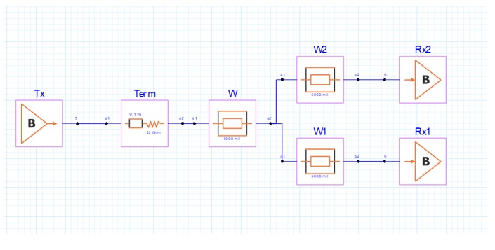
Taking a simple example, consider the clock distribution network for a series-terminated T topology. Exploration of the interface can begin before the schematic stage when the system block definition is defined.
Constraints can be captured to define the length between the driver and the series termination. Output driver impedance + resistance must match characteristic impedance of the main line. The resistor value and trace width can be swept to best match this case. Length can be swept for W1 and W2 to determine maximum length and matching requirements between the two traces.
After initial exploration, a key strategy in the schematic stage is to classify the design into classes of nets and create early exploratory analysis to derive constraints using what we have learned during the exploration phase. Once more design detail is provided, the initial test bench can be modified with additional detail including package models, connectors, and vias.
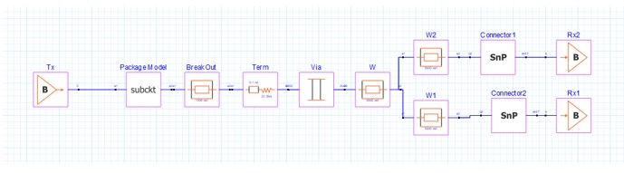
As data rates climb, additional attention needs to be paid to vias, which generally require the use of a full-wave solver. A via’s span (through, blind, buried), pad stack (i.e. hole/pad/antipad size), and proximity to ground vias all play a significant role in the insertion and return losses that are seen as “speed bumps” along the signal’s path.
This top-down methodology is well known, but there is room for improvement on basic 2D interconnect models. Engineering teams striving for ever-more accurate results can leverage existing design data with full-wave accuracy on realistic manufacturable CAD data. This underutilized process called virtual prototyping leverages a PCB layout tool to mock up structures. Put simply, virtual prototyping is a methodology to reuse existing design data to extract and simulate critical interfaces, such as these clock distribution networks.
Instead of importing massive netlists, layout tools can be started with a blank slate well in advance of the formal schematic. With an empty board created, a simple board outline can be drawn. Next define or import a stack-up and browse a few footprints from a CAD library or previous designs. This provides a basic floorplan from which to interactively define a few nets, representing the different critical classes of nets that will be in the next design. Route them with manufacturable traces and vias, and then define simple plane shapes.
This physical mock up would never be released to fab, but it can be used to provide representative physical structures to extraction tools, which in turn can produce detailed interconnect models to use in up-front simulations. Mocking up manufacturable structures in CAD software and then extracting this information assists in early identification of design tradeoffs. One does not need to be a routing expert to place existing part footprints and connect a few traces.
The aim of virtual prototyping is to closely match the end result of the finished layout by floorplanning components and routing in a PCB tool that is tightly integrated with simulation tools. Real trace and via models can be extracted with hybrid and 3D field solvers by mocking up classes of nets to get an idea of what the final layout can be.
Virtual prototyping allows designers to play in a sandbox during the exploration phase of the design, even with limited information. Everyone wants accuracy and complete systems, but shortcuts, place holders, and best guesses lead to good-enough answers early that can save time, especially when the testbenches are started pre-layout.