
As cellular and WLAN standards begin to transition towards next-generation performance requirements, such as 5G, the demand for high-speed radio frequency and microwave test equipment and interconnects will continue to increase. High performance radio-frequency (RF) connectors are utilized in a range of applications from RF/test measurement printed circuit boards (PCBs) to semi-conductor evaluation. Even through most RF connectors exhibit performance way beyond that of a conventionally fabricated PCB, the channel performance is directly dependent on their interaction with the board.
A particularly challenging configuration is the edge launch, where these connectors are used on the edge of the PCB with a transition to a microstrip trace. This transition zone typically consists of the interconnect, a coaxial structure landing on a pad, a planar structure, which then continues into a coplanar wave guide across the board. A poorly optimized connector footprint leads to degradation of the signal integrity performance, especially at high data rates.
This paper identifies the root cause of the problem by showing how the electromagnetic fields behave at the transition area. Then it demonstrates how to address these challenges by matching the size of the connector signal pin to the size of the top dielectric layer in the board. We address how ground discontinuities can be minimized with PCB modifications such as edge plating, milling, and castellated vias. Through the presentation of both simulated data, by utilizing a full wave 3D field solver software, and measured data, from our own connectors and boards, this paper exhibits the key dependencies between design variables and identifies the steps necessary to ensure the quality of high-speed data transmission. These results exemplify the direct relationship between overall channel performance and the interaction of the interconnect and board.
Example of Edge Launch Connector Application
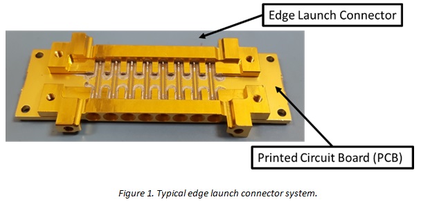
A typical application of an edge launch connector consists of a channel composed of a high-performance cable, a RF interconnect, and a PCB with the device under test (DUT). The transition from a cable to the PCB is accomplished by the RF connector, which must provide the necessary performance to ensure signal integrity throughout the entire channel. An ideal edge launch connector will provide a smooth impedance profile, minimize reflections, and have a robust mechanical connection. The connector footprint must be tuned to generate the desired performance. Close attention to the manufacturing process is also needed, specifically the solder process, to minimize ground discontinuities and any gaps between the connector and the PCB. A typical edge launch connector configuration is shown in Figure 1.
Identifying the Source of the Problem
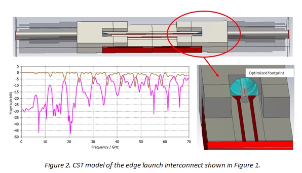
To identify the source of the problem, a model of the system shown in Figure 1 was simulated in Computer Simulation Technology (CST), as all models in this paper. This model consists of two connectors placed on opposite sides of the board, which also serves as a test board to characterize the performance of this connector. The mechanical representation of the connector has nominal dimensions with no ground discontinuities or gaps present between the connectors and the edge of the board. Figure 2 shows the model, together with the simulation results. We can see that resonances appear in the insertion loss profile. They are also matched by increases in reflections at those resonant frequencies. In the next section, several factors that can be leading to the degradation in performance will be outlined in further detail.
Field Leakage
To identify the source of the resonances, the 3D electrical field distribution at the transition zone between the connector and the edge of the PCB was generated. Figure 3 shows the field distribution at the edge of the board. It becomes clear that the electrical fields in this region are leaking below the first internal ground plane to the dielectric layer below. The field leakage translates to resonances in the insertion loss and, to make matters worse, the energy is coupling back on the other side of the board. The combination of these effects leads to a degradation in performance.

Ground Discontinuities
When moving from a simulation to manufacturing environment, a design engineer cannot assume the connector or board dimensions will be nominal. This requires a further analysis of both ground and signal discontinuities to identify any issues. To identify the source of the performance degradation, a RF connector was then simulated with different ground discontinuities. In this configuration, there is a sliding ground with a total of six contact points pressed by a spring to ensure a robust ground connection at the interface. An example is shown below in Figure 4, where an interconnect has many possible ground discontinuities.

These six contact points were removed systematically, and the simulations results were then compared to measured data. The resonances present in the measured data closely match the simulation results, where 50 percent or more contact points were removed. As expected, the resonant frequency is proportional to the size of the gap in the ground structure. The larger the gap is, the resonance is lower in the frequency spectrum. The results are shown in Figure 5.

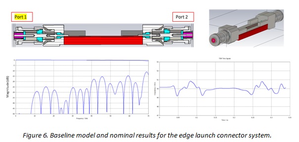
To investigate the effects of ground discontinuities in an edge launch configuration, we turn to the model shown in Figure 6. We incorporate manufacturing tolerances by making the mechanical dimensions deviate from nominal. There are four primary ground and signal discontinuities that were examined through simulation:
- The connection between the PCB co-planar ground structure and the connector ground: shown in Figure 7.
- The connection from the internal PCB ground plane to the connector ground: shown in Figure 8.
- The connection of the connector signal/inner pin to the PCB pad that it lands on: shown in Figure 9.
- The gap between the connector and the edge of the PCB: shown in Figure 10.
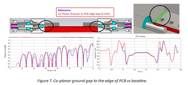
We begin with the connection between the PCB co-planar ground structure and the connector ground. In this case, the co-planar ground was pushed back 5-mil (0.127mm) from the edge of the board, resulting in a spike in impedance at the transition zone. This spike in impedance is not associated with any significant resonances, and the performance did not significantly degrade as the internal ground plane was the dominant effect in the ground structure. Figure 7 compares the results to the baseline model.
Next, a 5-mil gap was introduced between the internal PCB ground plane and the edge of the PCB. This creates a gap in the ground structure between the internal PCB ground plane and connector ground. The gap has two effects: a spike in impedance and a resonance around 25GHz. This also results in a spike in return loss at the same resonant frequency and in a general increase in reflections at high frequencies. Results are shown in Figure 8.

Another case shows the simulation results of creating a 5-mil gap at the signal trace from the edge of the PCB, which leads to a spike in impedance at the transition zone. This is expected as the signal pin transitions from being surrounded by an insulator (dielectric, Dk > 1) to air (Dk =1). This can be mitigated by bringing the signal pad all the way to the edge of the PCB, adding some capacitance to that region. Results are shown in Figure 9.


To prevent these discontinuities, the edge of the PCB must be as uniform as possible and can be milled and grinded down to place the copper as close to the edge as possible. These results also have some interesting implications, in that a gap in the internal ground plane and the edge of the board can be mitigated by the location of the coplanar ground relative to the connector ground. If the coplanar ground is close enough to the signal pin and connector ground, it will couple enough to prevent any further degradation in performance. Looking back at Figure 8, the performance degradation is limited by the presence of the co-planar ground structure.
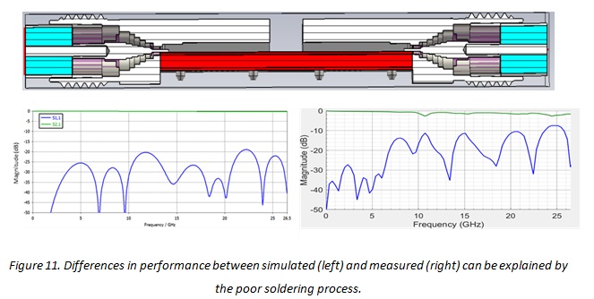
Another example of the effect of ground discontinuities in an edge launch configuration can be seen in the measured data shown in Figure 11. This edge launch connector did not undergo the correct soldering process as a solder stencil was not used. The performance substantially degraded in the measured samples, where the ground discontinuities lead to resonances and an increase in reflections across the frequency spectrum.
Matching the Size of the PCB Dielectric Layer and Connector Signal Pin
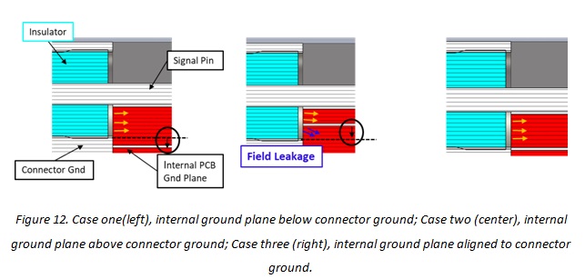
Edge launch connectors require proper alignment between the connector ground and internal PCB ground to prevent field leakage that will induce resonances and degrade performance. To further examine the electromagnetic field behavior in this region, three cases will be examined:
- Case one shows the internal ground plane lies below the insulator preventing field leakage, though a PCB dielectric layer that is very large compared to the connector will also degrade the performance.
- Case two represents what was simulated in the first model (Figure 2), where the internal ground plane is above the connector ground allowing the fields to leak through to the dielectric layer below.
- Case three shows a perfectly aligned connector ground to internal PCB ground. This is the ideal case as it prevents field leakage.
Figure 12 exemplifies the three cases.
Edge Plating (PCB)
Despite the importance of having a proper alignment between the connector ground and internal PCB ground plane, such a solution is not always possible. A connector with a large cross-sectional area may require a very thick top dielectric layer to place the internal PCB ground plane in the ideal location. Board real-estate is precious, and customers cannot always afford to dedicate a large section of the board to the RF connector.
Edge plating is a useful method to improve the performance when the ground structures are not aligned properly. By plating the edge of the PCB, no field leakage can occur to the dielectric layer below. In addition, ground discontinuities at the transition from the connector to the PCB are minimized or eliminated. The manufacturing process associated with edge plating and castellated vias is very similar to that of a via.
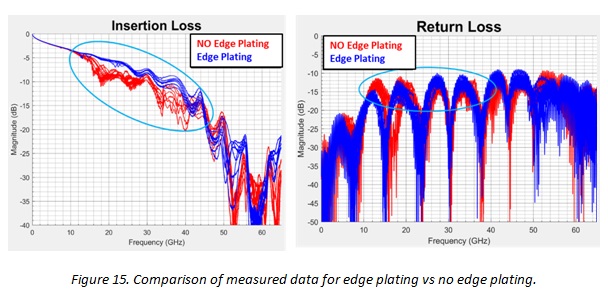
To evaluate the impact of edge plating, we included this PCB modification to the first model (Figure 2) to confirm whether the field leakage was reduced and prevented. The edge plating effectively prevented the field leakage to the dielectric layer below and increased the margin between insertion and return loss across the frequency spectrum. Figure 13 compares these new results to the original results without edge plating.
Finally, a large discontinuity in the ground structure is evaluated by adding a 5-mil gap to both the co-planar ground and the internal ground plane to the edge of the PCB, combining what we saw in Figures 7 and 8. The added gaps in the ground structure significantly degrade the performance by adding both reflections and resonances. Figure 10 demonstrated the results.

To continue examining the value of edge plating, a test board was manufactured in two variations: with and without edge plating. A connector with a large insulator and thus cross-sectional area was then soldered to opposite sides of the PCB. In this case, the edge-plated PCB left a column exposed where the connector is landing, which will reduce but not eliminate field leakage. Both connector/PCB assemblies were measured, and the data compared for further analysis. Figure 14 shows the boards utilized in this experiment.

The boards were measured using the Keysight PNA Network Analyzer N5227A 10MHz-67GHz and a 1.85mm standard calibration kit (85058B). The insertion and return loss for all eight channels are shown in Figure 15. As expected, the PCB with no edge plating had significantly more attenuation and resonances at high frequencies. The location of the resonances in the insertion loss matches the spikes seen in the return loss, which will reduce the channel margin. This correlates to the simulations presented in earlier sections where a misalignment in the ground structure leads to a degradation in performance.
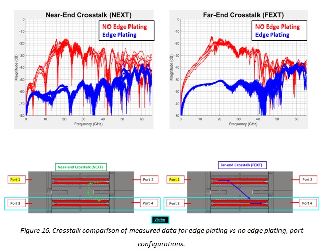
Furthermore, near and far-end crosstalk (NEXT & FEXT) were measured and compared as well. Figure 16 shows these results. There is a dramatic difference in performance between the edge plated and non-edge plated PCBs. The PCB without edge plating shows significantly higher crosstalk due to the increase in ground discontinuities present between the connector ground structure and the PCB ground planes. The ground discontinuities and misalignment of internal ground plane (relative to the connector ground) lead to field leakage and the radiation of energy, which translates to crosstalk.
In this paper, we identified the root cause of the edge launch resonances present in the PCB structure by showing how the electromagnetic fields behave at the transition area. Two different ways of addressing these challenges were shown: matching the size of the connector signal pin to the size of the top dielectric layer in the board and minimizing ground discontinuities with PCB modifications such as edge plating, milling and castellated vias. Through the presentation and correlation of both simulated and measured data, from our own connectors and boards, the key dependencies between design variables were highlighted. Moreover, a design methodology that ensures the quality of high-speed data transmission was outlined. These results exemplify the direct relationship between overall channel performance and the interaction of the interconnect and board.
This paper was originally presented at EDI CON USA 2018 and was an Outstanding Paper Awards finalist.