DDR memory interfaces are becoming increasingly common, and present a unique set of challenges to those designing high-speed embedded systems. This article will examine what DDR interface testing is all about, concentrating primarily on the physical layer and solutions to common problems.
Physical-layer tests ascertain whether the voltage levels, timing, and signal fidelities are adequate for a system to function correctly. This is distinct from protocol-layer testing, which determines whether the controller and memory chips are communicating properly at the digital level and above.
Within the domain of physical-layer test are three subcategories:
- Compliance: Do the device output signals comply with the JEDEC specfication?
- Validation: Do the devices interact correctly within the system environment?
- Debug: Why is my device/system not behaving as it should?
Compliance test means a raft of specific, mandated tests; these tests are critically important for DRAM and controller vendors. Validation tests, which are less prescriptive but require fuller visibility into system behavior, are critical for system integrators. Debug requires an exhaustive view of system behavior and typically follow from failed compliance tests and/or flawed system behavior.

Figure 1: Analyzing the interplay between the high-speed signals and the command bus deepens insight into DDR behavior
Which DDR signals are important for such testing? In physical-layer compliance and validation testing, the fastest signals shown in Figure 1 are the most critical: clock (CK), strobe (DQS), and data (DQn). These signals must be analyzed as analog waveforms to fully characterize their signal fidelity. And because there are many data lines in a DDR interface, testing all of them is a time-consuming proposition. Thus, in many instances, board-level simulation reveals the most likely worst-case data lines to isolate them for testing.
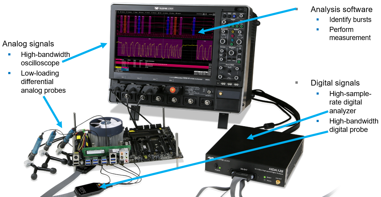
Figure 2: Shown is an example of a complete DDR analysis system
To gain a more complete system-level view, analyzing the interactions between the high-speed CK, DQ, and DQS signals and the slower command bus gives much deeper insight into behavior. In many cases, it is sufficient to acquire the digital state of these signals so long as the acquisition achieves high timing accuracy.
What would a complete DDR analysis system look like? Figure 2 provides an example. For acquisition of analog signals, a high-bandwidth oscilloscope is paired with low-loading differential probes. Digital signals call for a high-sample-rate digital analyzer and high-bandwidth digital probe. On the oscilloscope, analysis software handles identification of bursts and performs measurements.

Figure 3: Shown is a typical BGA package for DDR memory
Now let's look into some of the specific challenges one faces in a close examination of these interfaces.
The first test challenge is simply accessing the signals of interest. These days, DRAM chips come in ball-grid-array (BGA) packages that are wave-soldered to a matching array of pads on the PCB (Figure 3). How does one get to those pads?
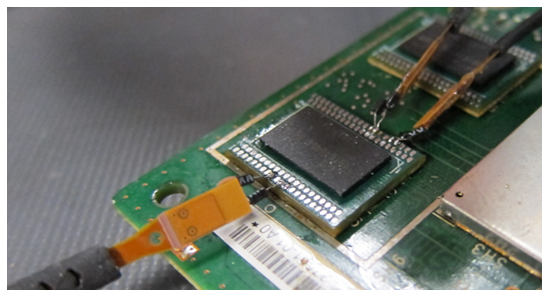
Figure 4: Interposers that sit between the DRAM chip and PCB can alleviate difficult signal access
Three common approaches to making BGA solder joints accessible include: backside vias, interposers, and DIMM series resistors. If they're included in the PCB layout, backside vias can be the ideal spot at which to probe DDR signals. Typically, good signal fidelity results from the vias' proximity to the termination. However, many devices, such as dual-rank DIMMs and dense embedded systems render this access option untenable.
The second option of interposers can also be useful in difficult access situations (Figure 4). As with backside vias, interposers afford reasonably good signal fidelity. However, they impose additional complexity if the socket is to be installed correctly. In addition, the interposer's footprint can be problematic on crowded PCBs.
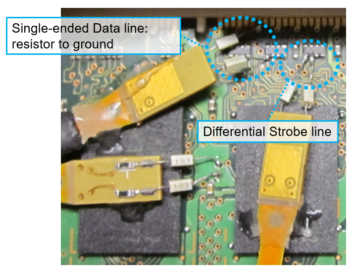
Figure 5: DIMM series resistors are a good alternative for dual-rank DIMMs
If dual-rank (or two-sided) DIMMs are involved, the backside vias won't be accessible. This makes DIMM series resistors a good alternate location for signal access (Figure 5). The downside of this approach is that the distance between the probe and the DRAM's terminations can result in problematic reflections from the receiver.
This content originally appeared on the Teledyne LeCroy Test Happens Blog.
See also: DDR Memory Interface Basics https://www.signalintegrityjournal.com/blogs/8-for-good-measure/post/473-ddr-memory-interface-basics