
The highlight event for me at the recent EDI CON 2017 was the High-Speed Digital Symposium, a conference within a conference. The theme of this three-hour event was how do we take information about the material properties of circuit board interconnects and integrate it into simulations to accurately predict channel performance?
Full disclosure, I was lucky enough to tag along with the invited speakers and moderate this group of industry experts, which included, as pictured in Figure 1: Al Horn, Rogers Corp, Brandon Gore, Samtec, Bert Simonovich, Lamsim Enterprises, Jason Ellison, Siemon Corp and Al Neves, Wild River Technologies. Here are some of the highlights from the presentations.
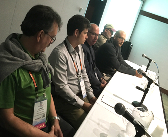
Figure 1. The panel of experts presenting at the High Speed Digital Symposium.
Brandon Gore, from Samtec, presented, Insitu Glass Fabric Characterization.
Glass weave skew is a difficult feature of a laminate to characterize because it is statistically based. This generally means having to measure a large number of traces to get a measure of the worst-case skew. Brandon presented a clever test structure design that guarantees finding the worst-case skew.
The structure is an array of seven and a half-inch-long, single-ended lines, probed from both ends. Each consecutive line is spaced 1 mil farther away from the next line than the previous adjacent line, illustrated in Figure 2. This means whatever the alignment of the first line to the glass weave, there is a high probability that one of the lines in the array will have been over resin rich and another line in the array over a glass reach region.

Figure 2. Each test line is 1 mil farther away from the next one as the previous one.
The min and max delays, measured from the unwrapped phase of the insertion loss at 14 GHz, represent the worst-case glass weave skew for that specific laminate structure. Looking at 1078 and 1035 type glass in Megtron6 laminate, he measured a maximum range in the glass weave skew of 5.07 psec/inch and 1.73 psec/inch, respectively.
Glass weave skew is really an issue for differential pairs. A common method to mitigate glass weave skew is to route the pitch of the differential pair on the same pitch as the glass weave yarn. This way, whatever environment one line sees, the other one will also see. This will dramatically reduce the glass weave skew sensitivity.
The worst case is to route the differential pair on a pitch that is exactly half the glass weave pitch. This guarantees that if one line is over the glass, the other one will be over the resin, the worst case. This is illustrated in Figure 3.

Figure 3. Routing the pitch of the differential pair on the glass weave pitch or half the glass weave pitch.
One of the test structures that Brandon included in his board was an array of differential pairs, one set of differential pairs with a pitch the same as the glass weave and another array with the differential pair pitch exactly half the glass weave yarn pitch. The difference in the delay skew distribution between the sets of differential pairs was striking. Figure 4 shows an example of the distribution of skews.
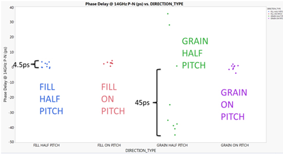
Figure 4. Impact on differential pair skew in 1078 glass yarn for a matched yarn pitch and 1/2 the yarn pitch.
(See the full video recording of Brandon’s presentation here)
Extraction of Frequency-Dependent Dielectric Constant: Loss and conductor effects of high-speed digital laminate materials for high-speed channel simulation, Allen F. Horn, Rogers Corp.
The test structures Al uses are microstrip traces on Ultralam 3850HT liquid crystal polymer (LCP) substrates. This is a low loss material with no glass so the features of the conductor loss can be more clearly observed. He’s built microstrip structures with different line widths and different copper surface treatments and roughness.
He’s been able to match model predictions of loss and delay based on measured roughness parameters using approximations and Sonnet simulations to VNA measurements up to 110 GHz. An example of his match is shown in Figure 5.
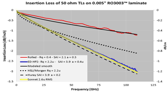
Figure 5. Measurement to model correlation for rolled copper and ED copper with 2.2 u rms roughness. Note the match with smooth copper and poor match above 25 GHz to the Hammerstad Jensen model roughness model.
The dispersion from the roughness, related to the capacitive loading of the dendrite features on the propagating wave, is fully taken into account in the full wave Sonnet model.
It is remarkable that rolled copper surfaces seem to match the modeled loss of ideal, smooth copper, with no roughness factor needed. The challenge, of course, is that while smooth copper sticks to LCP material, it doesn’t stick to many other laminate materials, especially low loss materials. Al alluded to a new material Rogers recently announced, RO1200 ELL (extremely low loss), to which smooth copper does stick well.
This combination of low loss laminate and rolled copper means the performance of channels made with this combination approaches the ideal behavior of smooth copper. Figure 6 shows the comparison of measured and calculated insertion loss to 50 GHz of microstrips with RO1200 and rolled copper compared to a simple approximation based on smooth copper and a Df = 0.001. It doesn’t get much lower than this.
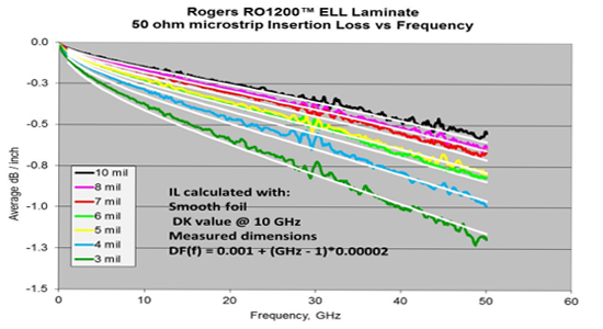
Figure 6. Measured RO1200 insertion loss with different line width microstrips compared to simple analytical approximations using smooth copper. The agreement out to 50 GHz is remarkable.
The combination of the low dissipation factor of RO1200 with the use of rolled copper which behaves like smooth copper is the ultimate, lowest loss system that pushes the fundamental limits to what is possible.
Test Vehicle Development for Systematic Development and Verification of Materials Models to 50 GHz (Signal Integrity), Al Neves, Wild River Technologies.
“What can possibly go wrong?” was really the subtitle to Al’s presentation. His company has built a series of well characterized test vehicles to correlate measurements and HFSS and Simbeor simulations to higher than 70 GHz. Based on these experiences, he reviewed his approach and some insights into what can go wrong.
He cautioned that when following his approach, there are some EDA tools that don’t correlate well above 16 GHz. Part of this is due to poorly designed text fixtures with structures that are either not de-embedded well, not captured in the 3D model, or use poor models of the dielectric and copper properties.
His approach is to use two different test structures. One structure is designed to test the design and modeling of the stack up. Every stack up has a bandwidth limit to it, based on the line widths of the conductors and the laminate selection.
When modeling a stack up, a cross section is a valuable tool to give confirmation of the dimensions which should be included in the 3D simulation. Having accurate values for the line widths and dielectric thicknesses increase the accuracy of the extracted material properties. He says the typically $2k cost of a cross section is well worth it.
His second test vehicle design is used to verify discontinuity structures such as the launches to the board and vias or pad stack ups to connectors or components. In order to de-embed a launch from a DUT structure on the board, the launch, including the coaxial connector, the pad stack, the clearance holes and even the residual stub, need to be engineered with an impedance discontinuity less than 1-2 Ohms up to the bandwidth required. If it is 4-5 Ohms, don’t expect accurate de-embedded results, he says. Generally, the measurement needs to extend above the frequency required, for accurate de-embedding. For example, when a 40 GHz de-embedded model is required, he will measure up to 50 GHz.
A Case Study of Effective Surface Roughness Acquisition, Jason Ellison, Siemon Company
It’s well known that smooth copper conductor losses increase with the square root of frequency and dielectric loss increases proportional to frequency. But, throw in copper roughness and the conductor losses increase faster than the square root of frequency.
Jason has explored using a simple analytical model to describe the total losses in a uniform transmission line using a power series expansion,
a = k1 x f0.5 + k2 x f + k3 f2
He calculates the coefficient values analytically using the Huray snowball model and the Hall and Heck model for causal inductance and resistance models. There is just one term to fit, the peak to peak copper roughness.
Measurements on Megtron 6 microstrip traces were used as the test vehicle. By sweeping the peak surface roughness term, the minimum in the error between the measured and calculated loss, gives the value of the roughness term. Figure 7 shows one example of the error term.
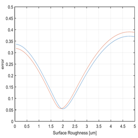
Figure 7. A minimum in the error between measured and simulation suggests the surface roughness is about 2.0 u.
The final test in this approach is comparing the analytical model for the total loss with the measured total loss, using just the Df and this roughness factor as parameters. Figure 8 shows this agreement out to 50 GHz. This is an example of another approach to modeling the combination of dielectric loss and conductor loss.
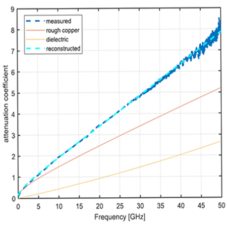
Figure 8. Final comparison between the measured total loss and the analytical approximation with the copper roughness term fitted to reduce the error.
Practical Modeling of High-speed Channels Based on Data Sheet Input, Bert Simonovich, Lamsim Enterprises
A common process to achieve good measurement to simulation correlation is to use a feedback loop, illustrated in Figure 9. In this approach, measurements on test vehicles are used to extract an empirical model which is then fed back into the simulation tool and the parameters are adjusted until there is a good match between measurement and simulation.
While this has the highest chance of success, and ends up with a model in the language the specific simulator uses, there isn’t necessarily any correlation between the parameters extracted and the intrinsic material properties. It also requires a high level of expertise, time and sometimes expense.
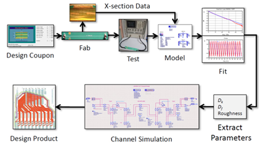
Figure 9. Feedback loop of the common approach to extract empirical parameter to use in a simulator to accurately predict channel performance.
An alternative approach to accurately predict channel performance is to start just with information available from a supplier’s data sheet. This is the simplest approach, and the lowest cost. But this approach only has value if it is accurate.
Bert presented a study that demonstrated it’s an achievable goal. The challenge is incorporating an accurate model for the impact on loss and phase delay from the copper roughness, and, as he points out, obtaining the right parameters to feed the model.
Some copper surfaces can have complex roughness texture, as shown in Figure 10.

Figure 10. Illustration of the copper surface texture in reverse treated copper foil.
He uses the Huray snowball model with his modification to feed it parameters based on stacking cannonballs. The material properties of the laminate come right off a vendor data sheet.
Starting with the vendor supplied maximum peak height of the copper foil roughness, he translates this into the snowball nodule size with his cannonball stacking model. From this he gets the parameters to use the Huray snowball correction to smooth copper loss, and includes the distributed capacitance loading to get the increase in Dkeff from roughness.
These are all the parameters he needs to include them in Polar Instrument’s latest version of their SI9000e simulator which calculates the S-parameters of a uniform transmission line based on cross section and material properties. It already incorporates the Huray model. The correlation between measured and predicted loss from the SI9000e tool is excellent, as shown in Figure 11.
![]()
Figure 11. Measured, in green, after de-embedding launches, of a uniform transmission line's insertion loss, compared with the SI9000e predictions, in red.
The final test is using this transmission line model, as part of a complete channel. Bert had designed a backplane evaluation board for FCI and compared the simulations of the complete channel based only on vendor supplied data sheets and the measurements of the complete channel. All the uniform transmission line segments came from the Polar SI9000e tool. Since he designed the vias, he engineered them to be very transparent. He didn’t even bother including the via models in the complete channel model. The connector models were as supplied by FCI.
The final comparison between the measured and predicted channel performance for a 20 inch long channel with 2 connectors, two daughter cards and a backplane segment, is shown in Figure 12. The agreement is remarkable. This is based on “dead reckoning,” with no fitting of any sort.

Figure 12. Comparison of the measured and simulated insertion loss and TDR response based on using only data sheet information as input.
Conclusion
Each of the five experts presented a different approach to incorporating material properties in simulations to accurately predict a channel’s performance. Along the way they each illustrated the same message, in different ways, that, as Dave Dunham from Molex is fond of saying, “above 10 GHz, everything matters.” While there are multiple approaches to achieve good measurement to simulation correlation, the complex behavior of the materials, especially the impact from copper texture, must be taken into account. There are multiple routes to achieve good predictive power, you just have to pay attention to all the details.