
High speed and portable electronics are still shrinking while power integrity demands continue to require lower power distribution network (PDN) impedance. Measuring sub-milliOhms is difficult. Getting low noise, sub-milliOhm measurements in very small circuits is a bit more difficult. We recently had the opportunity to support R&D Altanova [1] in performing this difficult measurement. We are grateful that they allowed us to use their measurement to help others facing this challenge. The final result, shown Figure 1, shows low noise even as low as 150 uΩ.
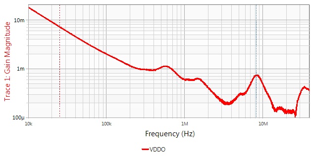
Figure 1 This off state measurement of the bulk caps and decoupling shows good fidelity even as low as 150uΩ. This is the final result.
The purpose of this article is to share some tips with you so that you can successfully perform these measurements, too.
Simulations generally come first
R&D Altanova is an expert at projects like this and uses simulation tools to optimize the PCB and decoupling before fabricating an expensive multilayer PCB. Simulation is a much faster, and less expensive method of optimizing the PCB decoupling than multiple circuit board revisions. The simulation results can also provide insight for the measurement setup as well.
The simulated VDDO PDN bulk capacitor and decoupling impedance is shown in Figure 2.

Figure 2 The VDDO power rail impedance without the VRM indicates the impedance is below 1 mΩ from 150 kHz to 40 MHz and less than or equal to 200 uΩ at several frequencies.
The PDN measurement setup
The simulation results show the impedance measurement range to be between 150 uΩ and 20 mΩ. The typical impedance ranges for the three S-parameter based impedance measurements are summarized in Table 1 [2]. Much of the impedance range falls below the recommended minimum, suggesting a difficult measurement, though the best option is the 2-port shunt thru measurement.
Table 1 High fidelity measurement ranges of VNA based impedance measurements.
|
Measurement |
Min |
Max |
Dynamic Range |
|
1-port |
1Ω |
2kΩ |
66dB |
|
2-port Series |
10Ω |
2.5MΩ |
108dB |
|
2-Port Shunt |
1mΩ |
225Ω |
108dB |
The measurement setup for the 2-port shunt thru measurement is shown in Figure 3.
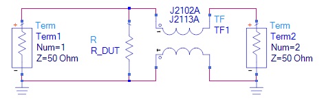
Figure 3 Typical 2-port shunt thru transfer impedance measurement setup showing the DUT, the VNA ports and the required coaxial transformer (see text)
The 2-port shunt through measurement includes an unwanted DC ground loop, due to the RF connection of the two port grounds at the instrument panel and the DUT ground connection located remotely at the DUT. This DC ground loop is well-documented [3] and is resolved by the introduction of a coaxial, common mode transformer as depicted in Figure 3. (Both passive and active off-the-shelf 50Ω matched coaxial transformers are available from Picotest.) The solid-state device yields the best performance, allowing measurement down to DC while the passive solutions are generally limited to several kHz. The active solutions are also usable to higher frequency than the passive solution.
Physical access is also a common limitation, with circuits continually shrinking and increasing in circuit board density. One good method of dealing with the physical aspect is to use UFL type micro-coax connectors rather than the more common SMA connectors. The UFL connector requires much less physical circuit board space as shown in Figure 4.
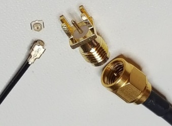
Figure 4 The UFL micro-cox connectors and lead wires require much less circuit board space than the more common SMA connectors. The micro-coax is a good solution for compact spaces.
The measurement setup, including the VNA, coaxial transformer (passive J2102A), connector lead-wires and the DUT, is shown in Figure 5.
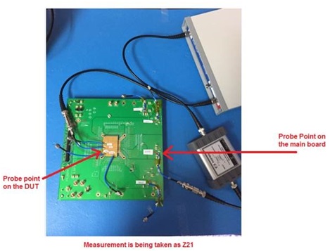
Figure 5 The 2-port shunt thru measurement setup, including the VNA, passive coaxial transformer (J2102A), connector lead-wires and the DUT. This particular circuit board is a 20 layer, Nelco N4800-20 PCB, 0.127” thick.
After calibration of the setup, an initial measurement is performed and the measurement result is shown in Figure 6. The measurement has the correct general shape, but for much of the frequency span, the measurement is significantly degraded by noise.

Figure 6 A first measurement attempt shows has the correct general shape, but the measurement is significantly degraded by noise.
Improving the signal to noise ratio
To be fair, this impedance magnitude is below the common recommended limit of 1millOhm. The S21 measurement at 150 uΩ is

And assuming the maximum +13dBm (1Vrms) source signal, the receiver signal is 6uVrms. The Bode 100, and most other quality VNA’s can measure a dynamic range of 104 dB and have a receiver sensitivity of less than 3 uV, so it is possible to make this measurement. Most VNAs, including the Bode 100, offer several methods of noise management. The five common methods are source amplitude, attenuators, receiver bandwidth, number of points, and trace averaging.
Source amplitude
In order to maximize the signal to noise ratio, it is desirable to set the source amplitude to the maximum level. This results in the largest signal at the receiver.
Attenuators
Attenuators reduce the signal and also add a finite amount of noise due to the attenuator resistors. If the DC voltage of the measurement is zero, then the CH2 port will likely not require any attenuation. It is possible that CH1 will require an attenuator, and the instrument will warn of a signal overload if this is the case.
Receiver bandwidth
The receiver noise is generally white noise with a finite noise density. The receiver noise is a function of the noise density and the square root of the receiver bandwidth. The narrowest receiver bandwidth results in the lowest noise, but this also corresponds to a longer sweep time, so consider the tradeoff between noise and sweep time, especially if you will be performing many measurements.
Number of points
The VNA, like other instruments required distinct datapoints. The trace is completed by interpolating between the datapoints. While the natural tendency is to increase the number of datapoint to reduce noise, this is often counterproductive. Fewer datapoint result in more interpolation, resulting in more “smoothing” of the data.
Trace averaging
Most VNAs, including the Bode 100, can also include trace averaging. The selected number of traces are averaged, reducing gaussian noise by the square root of the averaging depth. Like the receiver bandwidth, this comes at the expense of sweep time. An averaging depth of 10, for example, requires 10 sweeps to maximize the averaging. I rarely use this feature, mostly for this reason.
External options
There are also a few external options for improving the signal to noise ratio, including external signal amplifiers for both the source and the receiver ports and the cables themselves.
Source amplifier
The Bode 100 already offers a larger signal than many VNAs, but this can be increased using an external power amplifier. In many cases the VNA manufacturer offers signal source power amplifiers.
Receiver amplifier
The receiver signal level can be increased using a low noise preamplifer (LNA). Many companies offer LNAs, including Picotest’s J2180A with 2nV/rt-Hz input side noise density and 20dB signal gain.
Cables
Whether you use SMA or micro-coax connectors, choose cables carefully. Choose a cable with good shield efficiency, which often means multiple shield layers. These are available in both SMA and micro-coax forms. Also, get these cables from a quality manufacturer. Even a good shield cable can be compromised by a poor connector attachment. These cables do tend to be expensive, but with good care they’ll last a long time. Also, be careful how you dress these cables. Try to keep them away from noisy areas of the circuit board.
The improved measurement
Applying just a few of the noise management techniques can result in much better fidelity. The impedance measurement results using a 30 Hz receiver bandwidth, no attenuation on CH2 and 20 dB attenuation on CH1 are shown in Figure 7. The improved measurements are low noise even at the 150uΩ magnitude. Further noise reduction can be achieved by applying more of the internal and/or external improvement options.
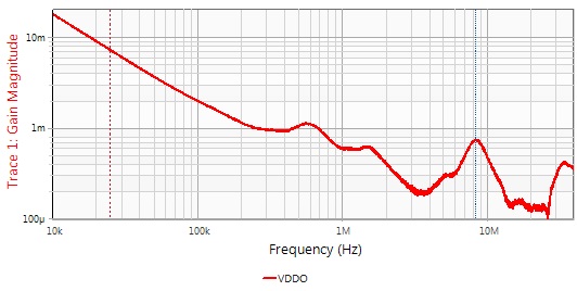
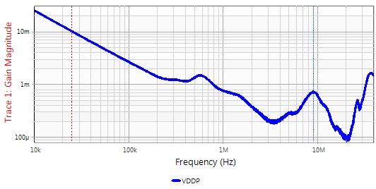
Figure 7 Reducing the receiver bandwidth, increasing the signal source amplitude and optimizing the attenuators results in much lower noise measurements.
Assuring the data is valid
There is always the remaining question regarding how we can be confident that the measurement is accurate. There are two recommendations for this. First, we can compare the measurements with the simulations. Agreement between the measurement and the simulation increases confidence in the measurement, however this does not guarantee the measurement is precise.
Another way to assure the measurement accuracy is to always measure a known quantity, and preferably in the same magnitude of the measurement you are making. For example, a mounted, 250 uΩ current sense resistor could provide a good indication of accuracy. Taken together, these two methods provide very high confidence in the accuracy of the measurement.
Comparisons between the measured results of Figure 7 and the simulation results are shown in Figure 8.
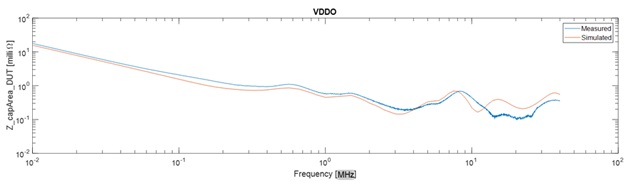
Figure 8 The VDDO measurement and simulation are in good agreement, resulting in a high confidence in the accuracy of the measurement results.
Conclusions
It is possible to perform accurate, low-noise impedance measurements even below 1 milliOhm. Numerous noise management techniques were presented, both internal and external to the VNA, and only several of them were necessary to achieve a reasonable fidelity measurement at 150 uΩ.
Special thanks to R&D Altanova for sharing their measurement and excellent correlations with us for your benefit.
[1] R&D Altanova is the leading provider of full turn-key test interface solutions specializing in Advanced Technology Printed Circuit Board Engineering, Design, Fabrication, Assembly and Manufacturing services. Technology solutions for the ATE industry include; fine pitch interface board fabrication, Burn-in Boards, embedded component solutions for interface boards and daughter-cards, Conductive Bridge™ and Coaxial Via™ technologies, elastomer interconnects and test sockets, as well as Signal Integrity and Power Integrity engineering and manufacturing services.
[2] S.M. Sandler, Extending the Usable Range of the 2-Port Shunt Thru Impedance Measurement, Microwave Conference (LAMC), IEEE MTT-S Latin America, 12-14 Dec. 2016, http://ieeexplore.ieee.org/document/7851286/
[3] S. Sun, L. D. Smith, and P. Boyle, “On-chip PDN noise characterization and modeling,” DesignCon, 2010