

Solver configuration
Initial probe-based simulations used the default conductor treatment and the default broadband analysis setup. Those runs provided a useful reference but did not correlate adequately with the measurement behavior. Two changes produced the strongest improvement.
First, Solve Inside was enabled for all conductors in the project. This allowed the computations to resolve the internal field and current distribution of the finite-conductivity probe bodies and in the vias, pads, and planes, instead of treating them as high-frequency impedance surfaces. Second, the adaptive analysis was changed from the initial broadband configuration to a single-frequency solution at 100 MHz, the chosen upper limit of the benchmark range. The converged 100 MHz solution was then used as the basis for the frequency-response comparison.
These changes matter because the probe is not merely a feed line attached to the DUT. At the very low impedance levels of the structure, current distribution and three-dimensional coupling within the access structure can be comparable to the response of the via field itself.
Results
After the adjustments discussed above, the results are interpreted as a configuration-specific correlation rather than as a search for a single universal J84 impedance. The role of the simulation is to reproduce the modeled measurement configuration faithfully enough that the remaining differences can be explained rather than hidden.
Three views of the response are used. Impedance magnitude on double logarithmic scale shows the “ birds-eye-view” or overall frequency-dependent trend. For all connection combinations, we expect a flat resistive response towards the low end of the frequency range, followed by an approximately straight upslope, representing inductive reactance. The inductance extracted from the imaginary part of the impedance isolates the portion of the result most sensitive to probe loops, via coupling, and current-path geometry. The resistance emphasizes the via cross section, conductor loss, and low-frequency offsets.
Impedance magnitude
Figure 7 compares the circuit-port baseline with the semi-rigid-probe configurations and the posted benchmark measurement data from Team 3. The comparison is done by plotting S21 magnitude, which is proportional to impedance magnitude. Note that the posted data from Team 3 intentionally includes the probes by having the calibrated reference planes at the probe input connectors, not at the probe landing points. The left plots refer to connections to the pads on the top, the plots on the right show the results with the connections to the pads on the bottom. The upper two plots show the correlation when the wafer probe is included in the simulation, the bottom two plots show the results with circuit-port excitation.
At low frequency, the response is governed primarily by resistance. As frequency increases, the inductive contribution becomes dominant and the curves become increasingly sensitive to probe placement and mutual coupling. The close and far cases show the size of that sensitivity without changing the underlying board geometry. This behavior is especially important for top-side probing, where the L2 short is close to the pads and the intrinsic via-path inductance is small. In that configuration, the probe loops can represent a substantial fraction of the total measured response. The longer bottom-side via path increases the DUT contribution and generally reduces the relative dominance of the same probe artifact [1].
The key result is not that an idealized port and a physical probe should produce the same curve. They should not. The useful correlation occurs when the probe-based model moves toward the measured behavior for physically defensible reasons and the remaining spread can be associated with known variables such as landing location, probe coupling, calibration, or contact repeatability.
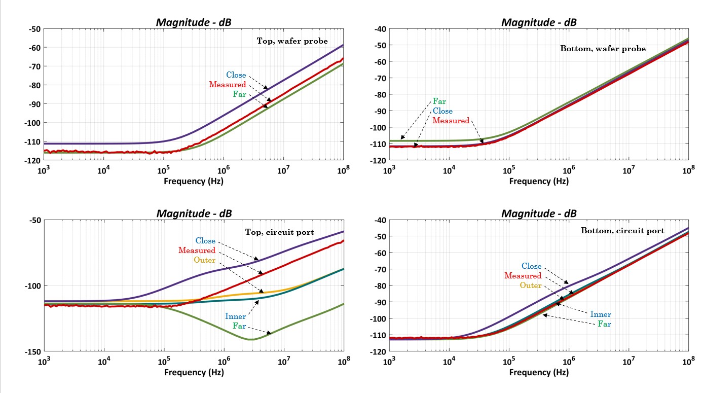
Figure 7: Impedance-magnitude comparison for the edge-port baseline and semi-rigid-probe configurations, with the benchmark measurement data included for correlation. The comparison separates the intrinsic structure response from the additional effect of the measurement access geometry.
Inductance
The shunt-inductance comparison in Figure 8 is the most direct indicator of three-dimensional effects, including the probe-tip loop coupling of wafer probes. The edge-port model establishes the inductive behavior of the reconstructed J84 geometry at the selected pad boundaries. Adding the probes introduces probe self-inductance, mutual coupling between the two probe structures, and coupling between the probe-tip loops and the vertical via loops.
These contributions can be of the same order as the J84 inductance itself. Their sign and magnitude depend on probe orientation and relative placement, which is why two plausible landing locations can produce a visible spread even when the board model is unchanged. The close and far cases should therefore be interpreted as a sensitivity band, not as numerical uncertainty. A model that ignores this band may appear simpler, but it omits one of the dominant physical error mechanisms in the measurement.
The improved probe-based correlation after enabling Solve Inside and using the 100 MHz adaptive solution supports the same conclusion: at ultra-low impedance, the conductor and field behavior of the probe model must be solved with sufficient fidelity. Treating the probes as incidental fixtures leaves too much of the measured inductive response outside the simulation.
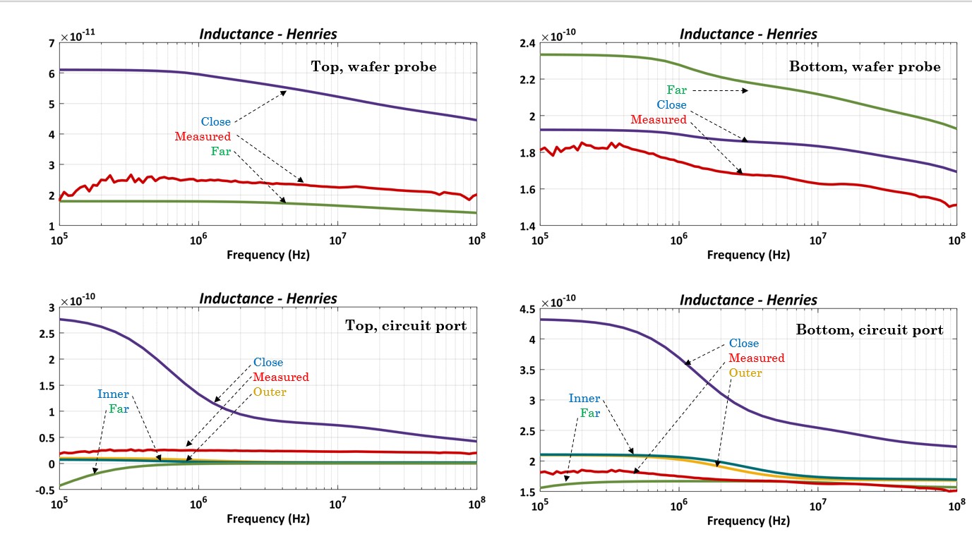
Figure 8: Inductance comparison for the edge-port baseline, semi-rigid-probe configurations, and benchmark measurement data. The spread among probe cases quantifies the sensitivity to three-dimensional probe coupling and landing position.
Resistance
Figure 9 isolates the resistive component of the complex impedance. This view is particularly important because it tests the geometric correction made at the beginning of the workflow. A solid imported via contains substantially more copper than the physical plated barrel and would therefore bias the simulated resistance downward. Reconstructing the correct wall thickness is a prerequisite for any meaningful low-frequency comparison.
The semi-rigid probe model also introduces finite conductor loss and a more realistic current distribution than the edge-port baseline. Enabling Solve Inside allows that contribution to be represented electromagnetically. Even so, a deterministic HFSS model does not automatically reproduce random contact resistance, probe pressure, oxide variation, or run-to-run landing repeatability unless those effects are explicitly modeled. Small low-frequency offsets should therefore be evaluated against measurement repeatability rather than interpreted immediately as a failure of the board model.
Taken together, the resistance and inductance plots provide a stronger diagnostic than impedance magnitude alone. If magnitude correlation improves for the wrong reason, one extracted component will usually reveal the compensation. The goal is a model in which the resistive and inductive trends are both physically consistent with the measurement configuration.
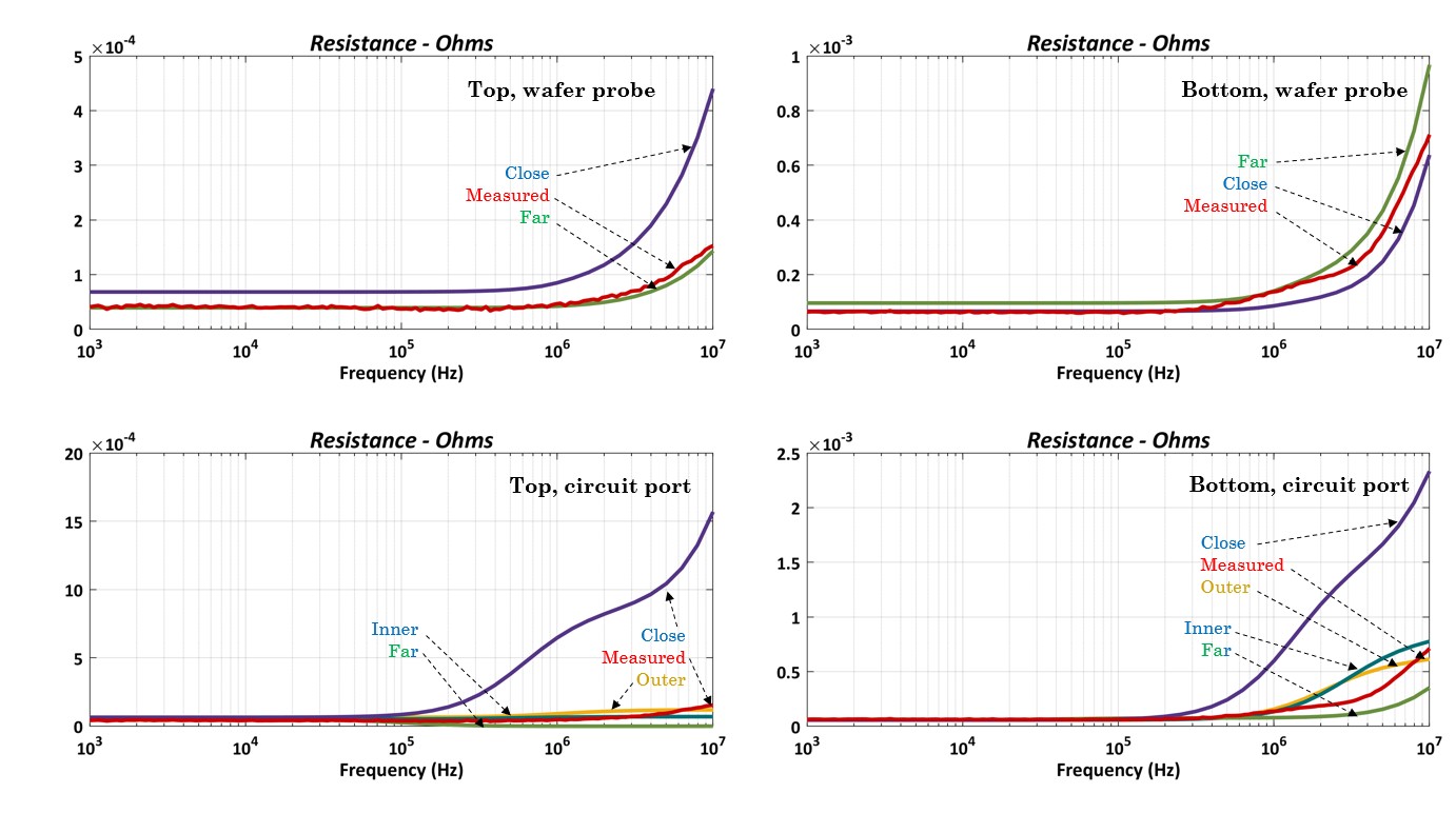 Figure 9: Resistance comparison for the edge-port baseline, semi-rigid-probe configurations, and benchmark measurement data. The plot tests the reconstructed via-barrel cross section and separates conductor-loss effects from the inductive behavior emphasized in Figure 8.
Practical implications for ultra-low-impedance correlation
Several practical conclusions follow from these results. Geometry must be verified before solver tuning; otherwise, numerical settings can be adjusted to compensate for a physically wrong model. Ideal ports are valuable for structural validation but cannot substitute for a three-dimensional probe model when the measurement includes significant probe interaction. Probe orientation and landing position must be defined reproducibly because they are part of the electromagnetic configuration. Finite-conductivity access structures require an appropriate conductor treatment, and adaptive meshing must be anchored to the frequency range in which the correlation is judged. Finally, the reported result should always identify its reference planes and access configuration rather than presenting one impedance trace as an access-independent property of the via field.
This interpretation is consistent with the purpose of Benchmark Problem V. The challenge is not merely to produce a low number. It is to understand which part of the observed impedance belongs to the via field, which part belongs to the way the structure is contacted, and which differences arise from measurement or numerical limitations. A useful simulation is one that makes those contributions separable and explainable.
Conclusions
Reasonable correlation of the J84 via-field challenge problem requires more than importing the board geometry and running a frequency sweep. The imported model must first be checked against the physical cross section and manufacturing geometry. In this work, the most important structural correction was replacing solid imported via prisms with hollow 16-sided barrels that match the measured outer diameter and wall thickness. Edge-based circuit ports then provided a necessary probe-free baseline that verified the reconstructed structure before measurement access effects were introduced.
The measurement-realistic stage added wafer probe models, finite contact faces, a controlled 45 degree approach angle, and repeatable close and far landing positions. Initial probe-based simulations showed that the default setup was not sufficient. Enabling Solve Inside for the probe conductors and changing the adaptive analysis to a 100 MHz single-frequency solution produced the strongest improvement in correlation. The resulting impedance-magnitude, shunt-inductance, and shunt-resistance comparisons show why probe geometry and solver treatment must be considered part of the electromagnetic problem at micro-ohm and picohenry levels.
The circuit-port excitation model establishes whether the DUT geometry is correct and provides a basic sanity check against gross errors in the setup; the probe-based model explains how the probe connection changes the observed response. Keeping those stages separate makes discrepancies easier to diagnose and prevents an apparent correlation from being achieved through compensating errors. The same approach can be applied to other ultra-low-impedance via arrays and PDN structures where the impedance of the access path is no longer negligible compared with the structure being measured.
Acknowledgements
Big thanks to Istvan Novak of Samtec for his mentorship throughout the simulation and documentation work. His guidance in troubleshooting, interpreting the benchmark, and refining the modeling approach was essential to the development of this publication. Special thanks to Janine Love of Samtec for her editing assistance. The author also acknowledges the help of several colleagues as well as volunteer members of the IEEE EPS Technical Committee on Electrical Design, Modeling and Simulation (TC-EDMS) for developing and making the Packaging Benchmark Suite available at packaging-benchmarks.org.
References
[1] "Power Integrity Via Field Impedance Challenge Problem V," IEEE EPS TC-EDMS, Apr. 7, 2026. https://www.packaging-benchmarks.org/repository/available
[2] "Introducing an Upcoming IEEE Packaging Benchmark," Signal Integrity Journal, 2024. https://www.signalintegrityjournal.com/articles/3430-introducing-an-upcoming-ieee-packaging-benchmark
[3] "Accuracy Improvements of PDN Impedance Measurements in the Low to Middle Frequency Range," in DesignCon 2010, Santa Clara, CA, 2010. http://www.electrical-integrity.com/Paper_download_files/DC10_12-TH3_Novak-Mori-Resso.pdf
[4] "3D Connection Artifacts in PDN Measurements," in DesignCon 2023, Santa Clara, CA, 2023. http://www.electrical-integrity.com/Paper_download_files/DC23_Paper_3DConnectionArtifactsinPDNMeasurements.pdf