

Ultra-low-impedance power distribution network (PDN) structures are difficult to correlate because the impedance of the device under test (DUT) can be comparable to artifacts introduced by probe coupling, probe landing, reference-plane placement, and electromagnetic solver configuration settings. This article shows some possible full-wave 3D simulation workflows for the IEEE TC-EDMS Benchmark Problem V, a four-via test case on 1 mm pitch in which the vias are shorted together on the L2 plane.
The workflow begins with exporting from HFSS 3D Layout to HFSS, corrects the imported solid-via geometry to match the measured via diameter and wall thickness values, and uses edge-based circuit ports to establish a probe-free baseline. Next, models of semi-rigid probes are added to the simulation geometry as the measured data includes the wafer probes without de-embedding. To represent the actual contact area, the conical probe tips are truncated, and a fixed 45° landing angle is used for the probes. We show that enabling Solve Inside for the probe conductors and anchoring the adaptive solution at 100 MHz produced the strongest improvement over the initial probe-based simulations.
Comparison of measured and simulated impedance magnitude, shunt inductance, and shunt resistance shows that accurate correlation requires the probe structure to be treated as part of the electromagnetic problem rather than as an afterthought.
Need for Modeling
As current demand rises and available routing area shrinks, package and PCB power-delivery structures increasingly rely on dense via fields. The impedance of these structures can fall into the micro-ohm and picohenry range, where effects that would be secondary in older PDNs can become comparable to the DUT itself. Probe-tip coupling, landing position, contact repeatability, reference-plane selection, current spreading, and numerical modeling choices can all shift the observed response.
IEEE TC-EDMS Benchmark Problem V was created specifically to expose these limits and to allow CAD and instrument vendors as well as system designers to use an open-source structure that removes confidentiality concerns in data exchange. The J84 test structure is deliberately simple: four plated-through vias on 1 mm pitch are shorted together by a single internal plane. Yet the benchmark does not define one universal value that every measurement and simulation must reproduce. The measured result depends on how the structure is accessed, and the benchmark therefore emphasizes understanding configuration-dependent behavior rather than forcing all methods to converge to a single nominal answer [1].
This study focuses on the modeling side of that problem. The objective is to build a workflow for Ansys HFSS 2025.R2 that first validates the physical structure independently of the probes and then adds the probe geometry. The method has four central elements: preserving geometry during export, reconstructing the via barrels to match the physical cross section, using edge-based circuit ports as an intermediate validation step, and introducing realistic semi-rigid probes with repeatable landing conditions and solver settings. The final comparison is made using impedance magnitude, shunt inductance, and shunt resistance because magnitude alone can conceal different combinations of resistive and inductive error.
Benchmark Structure and Correlation Objective
J84 is one reference structure on the larger benchmark board, which is described in [2]. J84 contains four plated-through holes on 1 mm pitch, with all four vias directly connected on L2, as shown in Figure 1. The board has six copper layers separated by five dielectric layers; the top and bottom layers are pad only. The benchmark focuses on low-frequency behavior up to about 100 MHz, where resistance and inductance dominate the response and dielectric effects are secondary.
The physical measurements use a two-port shunt-through configuration, a common approach for very low PDN impedance. Readers not familiar with it are referred to [3]. In large computing and communications boards access is often available only to one side of the populated board. This limitation forces same-side probing, and, as a result, the two probes interact electromagnetically with one another and with the via barrels. The relative importance of those interactions changes with probe orientation, landing position, and whether the structure is contacted from the top or bottom. In this benchmark problem, the top-side configuration is particularly demanding because the L2 shorting plane is close to the top pads, making the intrinsic via-path inductance very small and therefore more comparable to probe-loop artifacts [4].
For that reason, correlation is approached here in two stages. The first stage does a simple sanity check of the imported and reconstructed J84 structure, making sure it behaves approximately as expected when excited without physical probes. The second stage adds the actual correlation of the wafer probes and targets. This gradual approach helps to avoid failure modes in which probe errors, geometry errors, and solver errors are adjusted simultaneously, and the cause of an apparent mismatch becomes impossible to identify.
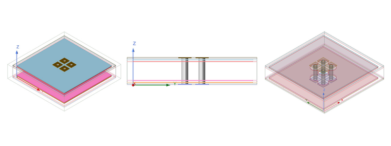
Figure 1: HFSS model of the J84 benchmark structure. Cross-sectional and oblique views show the four 1 mm-pitch plated-through vias, the top and bottom pads, the six-layer stackup, and the L2 plane that shorts the four vias together.
HFSS Model Import and Geometry Reconstruction
Exporting the board model from HFSS 3D Layout
The IEEE data port at [1] has the board CAD data in ODB++ format. It was imported into HFSS 3D Layout. A solution setup was added before exporting it to Ansys HFSS so that the vias and other curved geometries would be discretized consistently. As shown in Figure 2, in the General settings, vias were meshed as 3-D vias with 16 sides. In the Advanced settings, the arc step was set to 15 degrees and the maximum number of arc points was set to 16. The resulting design was then exported as an HFSS model.
These settings are not a cosmetic choice. Given the small size of the structure, the response is sensitive to small changes in geometry. Coarse faceting or inconsistent geometry during transfer can change both effective cross-sectional area and field distribution. Establishing the export procedure before any solver tuning prevents geometry conversion errors from being mistaken for electromagnetic correlation errors.
Figure 2: HFSS 3D Layout settings used before export. Vias were represented with 16 sides, the arc step was set to 15 degrees, and the maximum number of arc points was set to 16 before the design was exported as an HFSS model.
Reconstructing the physical via barrels
After export, the HFSS model contained the expected six copper layers, five dielectric layers, four centered vias, and top and bottom pads. Inspection of the via bodies, however, revealed a critical geometry error: the imported vias were solid 16-sided copper prisms rather than hollow plated-through barrels. The outer dimension was correct, but the missing bore added copper that does not exist in the physical board.
The measured cross section of the benchmark gives an overall via diameter of 371 µm and a wall thickness of 42 µm [1]. Each via was therefore corrected by creating a second, smaller 16-sided polygon with the same height and subtracting it from the imported via body. As shown in Figure 3, this operation formed the hollow barrel while preserving the imported outer diameter. The top and bottom pads were then restored at the correct elevations and thicknesses. Moreover, it is important to make sure that the pads are also hollowed.
This correction is fundamental to the low-frequency correlation. A solid via would overstate copper cross-sectional area, bias the resistance downward, and alter the way current crowds around the barrel and spreads into the shorting plane. In a structure whose target values are already in the micro-ohm and picohenry range, that error is large enough to invalidate later conclusions about probe behavior.
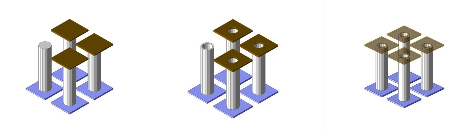
Figure 3: J84 via geometry correction. The imported model contains solid 16-sided copper prisms, which becomes visible when pads are hidden (left). The corrected model subtracts an inner polygon to form hollow barrels and hollow pads (center). The full corrected via structure is on the right.
Structural Validation with Edge-Based Circuit Ports
Before adding the geometry of the wafer probes, the structure with the corrected via barrels was simulated with circuit ports, which require excitation placed along edges of the structure. Out of the many possible permutations, the four shown in Figure 4 were simulated. The ports were assigned to opposing pad edges so that current entered the structure along defined paths. This provided a controlled excitation of the via geometry, but knowingly and intentionally ignored all contributors from the probes.
The purpose of this model was a simple sanity check, not direct measurement correlation. A circuit port at the pad boundary defines a different electromagnetic problem from a physical probe touching the pad. Its value is that it isolates the device geometry, making it independent of the probe connection. The resulting response provides a clean check of the low-frequency resistance floor and the transition to inductive behavior, while also confirming that the via barrels, pads, stackup, and L2 short are connected and meshed as intended.
Using this intermediate model makes later interpretation much easier. If the edge-port baseline is physically reasonable but the probe-based model disagrees with measurement, attention can be directed to the probe structure and solver treatment.
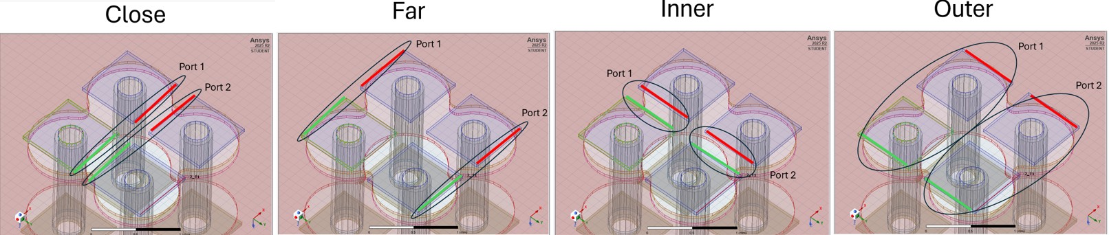
Figure 4: Edge-based circuit-port excitation used for simple sanity check. Ports on selected pad edges create a controlled, probe-free baseline before the probe structures are introduced.
Including Realistic Probe Model
Wafer- probe geometry and contact-face correction
The second simulation stage introduced semi-rigid probes to represent the physical measurement access with wafer probes. Each probe was modeled with its measured length (approximately 35 mm) and assumed nominal dielectric and conductor properties. The original probe model used a conical shape at the probe tips, ending in a sharp point. In a full-wave conductor model, that idealized point concentrates current into a vanishing area and can create a numerical singularity that has no physical counterpart in the measurement.
The probe tip was therefore truncated at the intended contact location to create a landing face with finite area, see Figure 5. This modification preserved the overall approach geometry while providing HFSS with a realistic contact area and a bounded current-density distribution. The probes were then oriented at 45 degrees relative to the pad surface to match the measurement setup as closely and repeatably as possible.
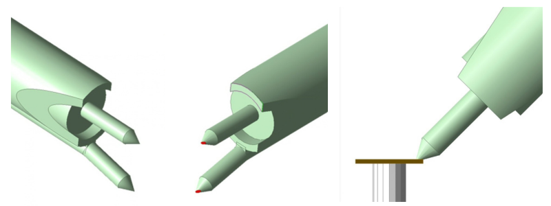
Figure 5: Wafer probe model with ideal geometry (left-most image) and after correction (in the middle) to create realistic contact area, highlighted in red. The probes are positioned at a 45° approach angle. On the right a side view is shown with the corrected probe tip landed on the pad.
Repeatable close and far landing positions
Probe landing is not a minor detail in this benchmark. The pads are intentionally large enough and square shaped to allow the use of different probe pitches and contact locations. Each of the different probe pitches and landing locations creates its own specific current path on the pads as well as different coupling between the probe tip loops. Exhaustively sweeping every possible landing point would be computationally expensive and would make the comparison difficult to interpret. Instead, two deterministic landing conditions were used. As shown in Figure 6, in one extreme, called the far position, shown on the left two images, the probe contact was placed midway between the outer pad edge and the via perimeter. The opposite extreme, called close position, shown on the right images, used the same offset convention but referenced the contact toward the via. The same modeling logic was used for the top-side and bottom-side configurations.
The close and far cases are not intended to identify one universally correct contact location on the pad. Instead, these practical extremes were used to quantify and illustrate the sensitivity of the modeled result to a realistic range of probe placement. This is consistent with the benchmark objective, which treats probe position and three-dimensional probe interaction as part of the correlation problem [1].
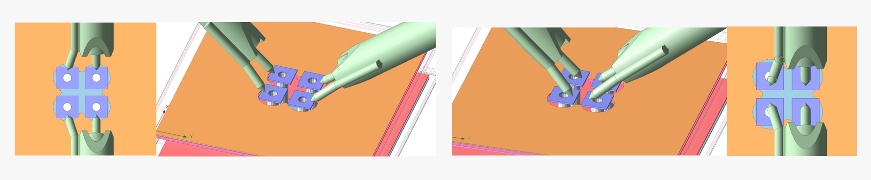
Figure 6: Probe landing positions. The far and close conditions provide repeatable reference locations for evaluating sensitivity to probe placement without an impractical exhaustive sweep of the pad surface.