

PCIe 7.0 Readiness and PCIe 6.0 CEM Validation, with a Path to 256 GT/s
Introduction: PCIe 7.0 Readiness and the Path to 256 GT/s
PCI Express® is accelerating to meet AI and hyperscale infrastructure demand. PCIe 7.0 reached Base Specification release in June 2025, defining performance at the ASIC pins, and the Peripheral Component Interconnect Special Interest Group (PCI-SIG) Board also announced direction pushing PCIe to 256 GT/s, signaling an accelerated roadmap beyond PCIe 7.0 128 GT/s, and reinforcing a faster standards cadence than prior generations. This shift is not only about higher throughput. As electrical margins shrink employing PAM4 signaling, channels become more challenging, and common form factors such as motherboard and add-in card (Card Electromechanical or CEM) implementations remain central to deployment.
Why the PCIe Roadmap Is Accelerating
PCIe is doubling its bandwidth with each new generation, but the gap between significant specification versions has narrowed in recent versions. The reality is that AI, high performance computing, and data centers require massive bandwidth. The industry is looking for faster ways to move AI models and inference data between CPUs, GPUs, network cards, and storage drives. As seen in Figure 1, PCI Express bandwidth scaling from early PCIe implementations in the early 2000s at ~2.5 GT/s to PCIe 6.0 at ~64 GT/s and PCIe 7.0 at ~128 GT/s.
Compute performance needs to keep up with next-gen Ethernet and accelerators, which push the need for higher system bandwidth using wide links utilizing numerous lanes, especially x8 and x16 lane widths. For that to occur, PCIe lanes need to be as fast as physically possible. In addition, hyperscalers are requesting faster link bandwidth and are ready to deploy these technologies as soon as they are available. Because of this massive demand, new PCIe standards are accelerating to keep pace with the interconnect needs of modern AI workloads.
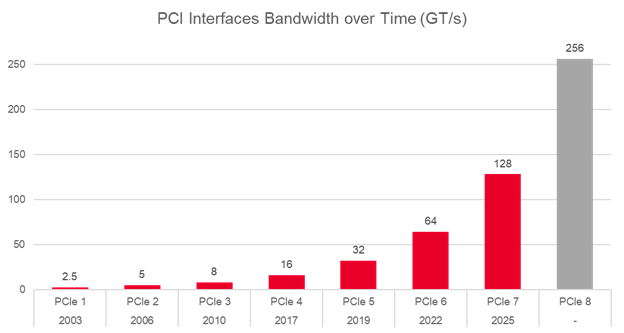
Figure 1: PCI Interface Bandwidth Growth Over Time
Technology Evolution: From Open Eye to PAM4
In the early generations of PCIe, the specs were built around the transmitted signal having an "open eye", meaning the signal arrived at the receiver clean enough to be converted to a data stream at the target bit error ratio (BER). But as speeds increased, the signal began degrading in the channel, and equalization became necessary. Since PCIe revision 3.0, the PCIe specification assumes the channel is completely "closed" and unreadable without both transmitter and receiver equalization.
To keep pace with bandwidth demands without doubling the physical lane count, PCIe 6.0 technology introduced PAM4 signaling (two bits per symbol, compared to one bit per symbol with NRZ). The PCIe 7.0 specification continues with PAM4 and doubles the data rate to 128 GT/s by increasing the PAM4 symbol rate to 64 GBaud.
While PAM4 enables higher throughput, it introduces additional signal integrity and measurement considerations:
- Compressed vertical margin: NRZ (PAM2) uses two voltage levels and one eye. With a total swing of voltage V, the eye height is roughly equal to V at the transmitter pin. PAM4 uses four voltage levels and three stacked eyes. Keeping the same total swing V, each eye is about V/3. That reduces voltage margin by 1/3, giving an SNR penalty of ~9.54 dB. This makes PCIe 7.0 more sensitive to crosstalk and jitter.
- Reduced horizontal margin: Unit Interval (UI) is the symbol time. NRZ transitions are full-swing; PAM4 includes many small-step (1-level) transitions (for example, L1 → L2) that move only 1/3 of the voltage distance. Those smaller steps have lower effective slew rate (dV / dt), so they cross receiver symbol thresholds more slowly. With Inter-Symbol Interference (ISI) and jitter, the slow edges lose proportionally more timing margin. Practically, the usable horizontal eye opening can shrink by about ~33% versus ideal NRZ under similar conditions.
- More complex analysis: PAM4 jitter validation can no longer rely on a two NRZ edges relative to the recovered clock edge; it requires multi-level, transition-aware analysis to capture level-dependent jitter, distortion, and linearity effects) comprehending 12 total edges.
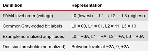
Table 1: PAM4 Level Definitions and Decision Thresholds.
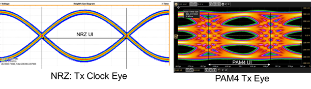
Figure 2: PAM4 incurs ~9 dB SNR loss vs NRZ because one eye becomes three smaller eyes. Slower adjacent-level transitions also reduce the usable timing window
- Routing discontinuities consume meaningful margin
- Connector transitions become large loss contributors and generate reflections
- Via stubs can quickly consume the available margin due to impedance changes.
PCIe 7 introduces much stricter routing constraints, tightening the total pad-to-pad channel loss budget to approximately −36 dB at 32 GHz (as shown on Table 2). Practically speaking, this sets a baseline for hardware engineers: PCB traces must now be designed to exhibit less than 1.0 dB of insertion loss per inch (2.5 cm) at nyquist.
At 32/64 GBaud PAM4 in PCIe 6.0 and PCIe 7, electrical margin becomes razor thin, requiring test methods to distinguish true silicon behavior from channel and measurement artifacts. PCIe 7.0 channels can drive the received PAM4 top eye (opening between L2 and L3) into the single-digit millivolt range, pushing validation into a measurement sphere where noise, distortion, and small nonlinearities dominate the error budget. As a result, metrics such as signal to noise and distortion ratio (SNDR -minimum 34 dB), 12-edge jitter (with Tx uncorrelated total jitter capped at a maximum of 2.0 ps peak-to-peak), and transmitter level linearity (Level Separation Mismatch Ratio, RLM) (minimum 0.95) become difficult to achieve, alongside filtered reference-clock phase jitter limits that have now shrunk to 67 femtoseconds RMS (filtered).
Backward compatibility isn't just an electrical compliance issue; the mechanical connector is another topic to consider, given the installed base. The original CEM connector was not originally designed with 128 GT/s throughput in mind. Trying to keep that legacy connector form factor while hitting PCIe Gen 7 speeds has forced the connector vendors to investigate innovative design and manufacturing techniques to meet the PCIe 7 CEM channel requirements.
The PCIe Base Specification is based on a die pad to die pad channel reference, while the CEM specification defines performance at the CEM connector. CEM form factor products remains one of the most widely deployed PCIe implementations. Nevertheless, the CEM specification remains fundamentally dependent on the requirements of the PCIe BASE specification.
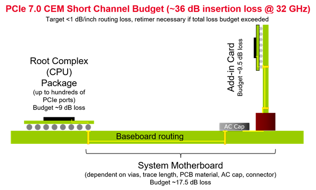
CEM validation is harder than package-level validation because motherboard traces and connector transitions are far more lossy and reflective compared to silicon electronic validation (EV) fixtures for integrated circuit devices
To improve repeatability in harsh channels, PCIE 6.0 CEM testing for TX signal quality has shifted toward a statistical eye calculation methods that combines:
- A step response characterization of the transmitted preset signal (for example, SigTest-type offline signal-analysis)
- A statistical simulation and eye rendering process applying PCIe 6.0 reference equalization (Seasim statistical channel simulator style) to render the compliance eye from characterized channel behavior.
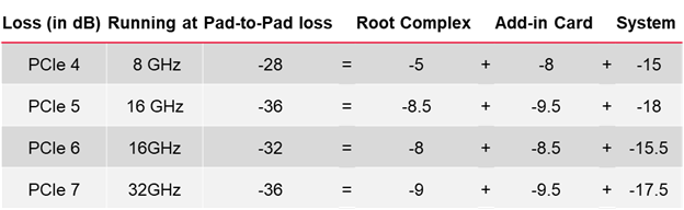
Table 2: Pad-to-Pad Channel Loss Allocation by PCIe Generation
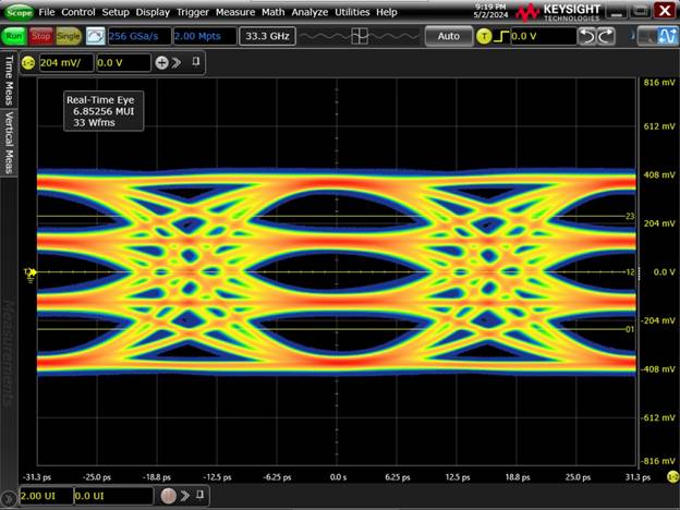
Figure 4: Example PAM4 eye diagram at high data rate under ideal short channel conditions. In actual systems, you will likely never see a PAM4 eye this open, especially without extensive equalization.
Reliability Framework Behind PAM4
When PCIe 6.0 introduced PAM4 and forward error correction (FEC), it laid the groundwork for the massive 128 GT/s speeds the industry is now experiencing with PCIe 7.0. But as these speeds increase, it is arguably the physical electrical layer, more than protocol or software, that’s causing the most headaches during bring-up. At the end of the day, physical realities like link margin, signal loss, and noise are what actually determine whether a design will successfully train an AI model and remain stable under a heavy workload.
At 64.0 and 128.0 GT/s, the PCIe 7.0 specification mandates Flow Control Unit (FLIT) mode to maintain required link BER performance with PAM4 signaling. By spreading that overhead across a larger 256-byte unit, FLIT mode maximizes available bandwidth. A fixed-size 256-byte FLIT (unchanged from PCIe 6.0) contains:
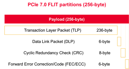
Figure 5. PCIe 7.0 FLIT partitions (256B).
Because PAM4 yields a significantly worse raw BER than older NRZ generations, the electrical requirement of FBER < 10⁻⁶ acts as a pre-FEC target to ensure a highly reliable post-FEC FLIT outcome. The fixed length of the FLIT is a requirement for the forward error correction (FEC) critical to meeting a 10-12 BER in the PCIe 7.0 link.
Reference Receiver (RR) and Core Electrical Metrics
When data is moving at 64 or 128 GT/s, evaluating whether a receiver can decode those channel degraded PAM4 signals comes down to a two-pronged approach: relying on the silicon's built-in diagnostics and constrained-compliance models.
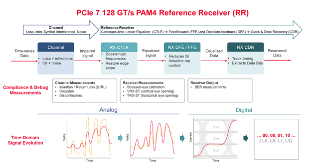 Figure 6: The PCIe 7.0 128 GT/s PAM4 Reference Receiver (RR) signal conditioning chain.
As part of compliance, the core transmitter tests required for PCIe 6.0 remain mandatory for PCIe 7.0 devices. They validate that silicon is actually generating a clean, compliant waveform at the physical layer, rather than just passing logical checks at the protocol layer. These carry-forward measurements include:
- TX de-emphasis and package loss characterization
- Pulse-width jitter (PWJ)
- Clock phase jitter
- Return loss
- All lower-speed TX validation (below 64 GT/s) for interoperability across legacy rates and equalization states.
To validate PAM4 margins at 128 GT/s, PCIe 7.0 had to introduce additional transmitter compliance requirements. The focus now is heavily on waveform quality and strictly controlled test environments.
- PAM4 Waveform Quality Metrics: To understand where margin erosion is happening, advanced metrics are necessary, such as SNDR, multi-edge jitter analysis, level separation mismatch (RLM), and the new AC-method preset tests (0-10 presets).
- Controlled Lab Topology: Isolate the silicon's behavior from the artifacts generated by the test fixtures (within the allowed limits defined for specific TX tests). Usually, this means using custom breakout boards, a low-jitter reference clock, specific replica channels, and CTLE-based compensation.
Jitter requirements tighten from Gen6 to Gen7: the target first bit error rate remains 10-6, while uncorrelated jitter budgets are roughly halved to preserve margin at 128 GT/s.
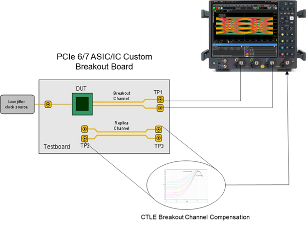
Figure 7: PCIe 6.0/7.0 PAM4 transmitter test setup. For jitter measurements only, CTLE equalization may be applied to compensate for the channel effects of the breakout board.
As link speeds increase, minimum instrumentation requirements rise as well. PCIe 6.0 specifies a minimum real-time oscilloscope bandwidth of 50GHz for transmitter characterization. The PCIe 7.0 specification increases the minimum oscilloscope bandwidth to 65 GHz, with the higher bandwidth providing headroom for pathfinding and correlation.
The oscilloscope capture illustrates the practical spectral realities of a 128 GT/s PCIe 7.0 PAM4 signal and shows why extended bandwidth is required for trustworthy measurements. In the frequency domain, the first harmonic energy lobe extends to the 32 GHz Nyquist point, where the signal first shows a reduction in frequency content. But the signal doesn’t simply disappear after that. There is significant high-frequency content driving the signal up to the second harmonic or 64GHz. You want enough bandwidth in your real-time oscilloscope to capture both the first and second harmonic energy when characterizing your transmitter or performing the calibration of the pattern generator output for receiver testing.
This matters because a measurement system limited near 32 GHz would attenuate the higher-frequency components that shape edge placement and level transitions, effectively filtering out information that directly impacts jitter, SNDR, and linearity results.
Treat oscilloscope and BERT as a paired workflow: scope-driven calibration, analysis, and de-embedding, with BERT-driven stress and BER validation.
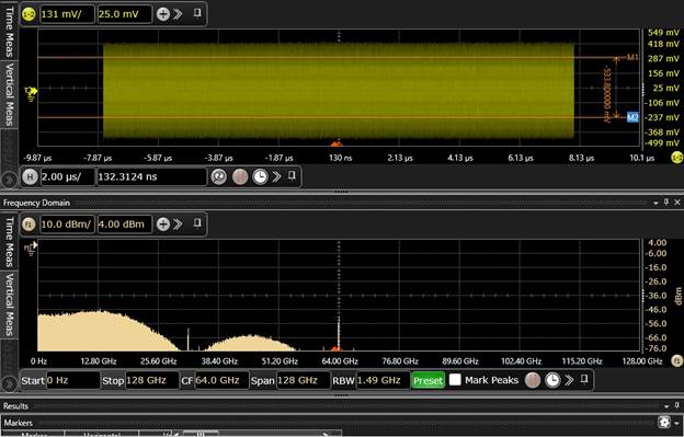
Figure 8: Time and frequency domain captures of a 128 GT/s PAM4 signal.
Conclusion
PCIe’s speed roadmap is being pulled forward by AI and hyperscale systems that demand more bandwidth per link, and that demand is accelerating. Success at these speeds will be determined less by the headline data rate and more by disciplined, end-to-end validation while paying close attention to channel margin and connector behavior. Keysight supports this lifecycle with a complete PCIe 6.0 and 7.0 solution set spanning simulation, interconnect characterization, transmitter compliance, stressed receiver testing, and protocol debug.