
For designers of integrated circuits and circuit boards, electromagnetic emissions are a critical concern. Designers need to ensure the final products comply with international standards for controlling radiated emissions. They must also ensure that a product does not cause self-interference or interference with other devices when part of a larger system. If electromagnetic interference (EMI) and electromagnetic compatibility (EMC) problems are not detected and fixed early in the design process, the consequences can include production delays, missed time-to-market goals and higher costs. To correct EMI and EMC problems early, they must be identified before compliance testing, with detailed information that standard far-field compliance testing cannot provide. Far-field measurements indicate whether a device has passed or failed, but they do not add much value for discovering the root cause of an emissions issue. For this reason, very-near-field tools capable of pinpointing problems are essential; the faster and more accurate the tools, the better.
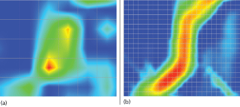
Figure 1 EMxpert ERX+ spatial scans at levels 1 (a) and 3 (b).
Most available tools emphasize high speed or high precision, not both. A traditional handheld probe is useful for finding sources of emissions, yet it doesn’t provide an overall picture of the board and can miss potential sources of emissions. Robotic positioners will individually scan all the features where emissions might occur and with high precision, but they can take hours. A much faster method is using a scanning array that applies multiple probes simultaneously, enabling the user to measure an entire board or section in less than a second. Not only faster, a scanning array is repeatable.
THE BEST OF BOTH
A new scanning technique is available that delivers both speed and accuracy, with the ability to precisely pinpoint emissions in just minutes, even from inside an integrated circuit or microchip. The EMxpert™ ERX+™ from EMSCAN™ provides higher resolution by combining a 1218-probe array with a fine and precise mechanical motion. A robotic positioner moves the entire array methodically to fill in the distance between probes. This technique increases the density of points measured—up to 65,000x the number of points—by dividing the scanned area into tighter and tighter grids according to user settings (see Figure 1). The ability to increase density makes a significant difference in the resolution of the spatial image provided by the scan. For example, changing from a level 1 scan to a level 8 scan, the highest density setting, reduces the effective spacing between measurement points from 7.5 to just 0.06 mm. Details of small features become available, even inside components.
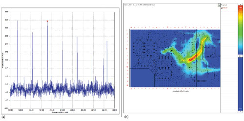
Figure 2 Spectral (a) and spatial (b) views of a scan.
The EMxpert ERX+ enables quick sampling of the magnetic field distribution of a product, with a visual display of the results. An embedded spectrum analyzer with intuitive visual imaging provides both a spectral view, to identify the frequencies of emission, and a spatial view, to visualize location (see Figure 2).
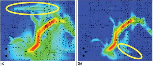
Figure 3 Energy coupled onto power plane (a) and control line (b).
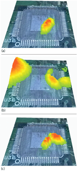
Figure 4 Views of IC emissions at 100 (a) 120 (b) and 130 MHz (c).
A quick scan typically identifies many emissions. The EMxpert ERX+ software allows the scan to “jump around” the board, zoom in and isolate emissions by location or frequency. Overlaying a design file or image of the board on the spatial view makes it easy to correlate the energy shown in the display with specific circuit board features, such as ICs, power planes and control lines (see Figure 3). For multilayer boards, multiple layers can be displayed to follow emissions coming from a trace that starts on one layer and continues deeper. If currents move to an internal layer that is shielded, there will be no fields in the external environment for the EMxpert ERX+ to measure. In this case, the currents are not relevant to a radiated emissions problem. If the shielded feature is the root cause of emissions leaking out of holes in the shield or at the board edge, the scanner will be able to measure it.
INSIDE AN IC
The extremely high resolution of the EMxpert ERX+ enables it to peer inside an IC and isolate the radiation from individual pins and wire bonds at various frequencies. Spectral and spatial views can be combined to provide a three-dimensional image of the emissions. Looking inside an IC, it is possible to see the sources of radiation, whether they are coming from the die region, from pins on the IC or spilling onto the IC from a different portion of the board (see Figure 4). Using this information with knowledge of the IC design, the user can solve the emissions problem.
The capabilities provided by EMxpert ERX+ add up to faster time-to-market, reduced project cost and increased productivity. EMxpert ERX+ presents real-time scans in seconds that identify spurious and continuous EM emissions. It provides spatial and spectral scans that allow design teams to cut one to two design cycles out of product development. It also reduces EMI testing time by up to two orders of magnitude. EMxpert ERX+ enables scans to be conducted where designers are located, obtaining results in minutes. Testing a new design in a third-party chamber could require traveling to an offsite test facility for the day, after potentially waiting days or weeks for a chamber to become available. The spatial and spectral scans provided by the EMxpert ERX+ system improve the ability to document new features and can be key elements in product marketing, giving customers graphic proof of a product’s EMI characteristics.
EMSCAN
Calgary, Alberta, Canada
www.emscan.com