
Introduction
Coupled microstrip lines exhibit strong far-end crosstalk (FEXT) due to unequal phase velocities of the even and odd propagation modes. The diagram in Figure 1 shows that, in the case of the even-mode, a larger portion of E-field is travelling in the substrate material and therefore the effective dielectric constant is greater compared to the odd-mode dielectric constant
  . The characteristic impedance of the even-mode
 is larger than the one of the odd-mode
 as well. This is because the characteristic impedance is defined as
 in the lossless case
 series inductance per unit length,
 shunt capacitance per unit length). Reduction of microstrip FEXT has been addressed in high-speed digital design by the use of stubbed transmission lines1,2 or dielectric overlays3. This phenomenon also plays an important role in microwave engineering, as microstrip coupled line backward couplers suffer from poor directivity when not compensated. Techniques to improve directivity are similar to those for high-speed digital design and include dielectric overlays4, the use of wiggly lines5,6 and capacitive compensation7,8,9. Reference 8 proposes equations for the calculation of optimum capacitance values for compensation. However, it requires the modification of the dimensions of the coupling structure itself. In this article, a more general approach, which does not require a modification of the dimensions of the coupled line structure, is presented, and closed form solutions for optimum capacitor values are provided
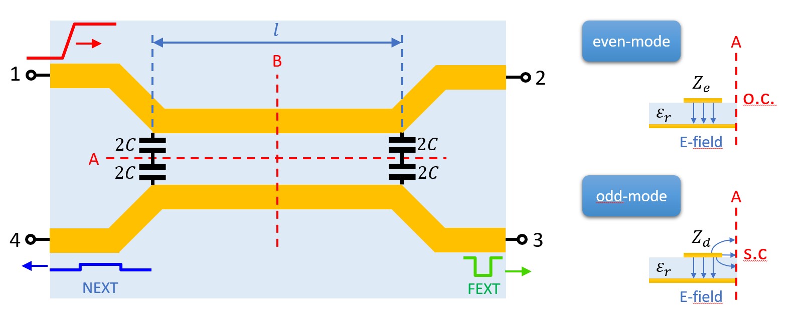
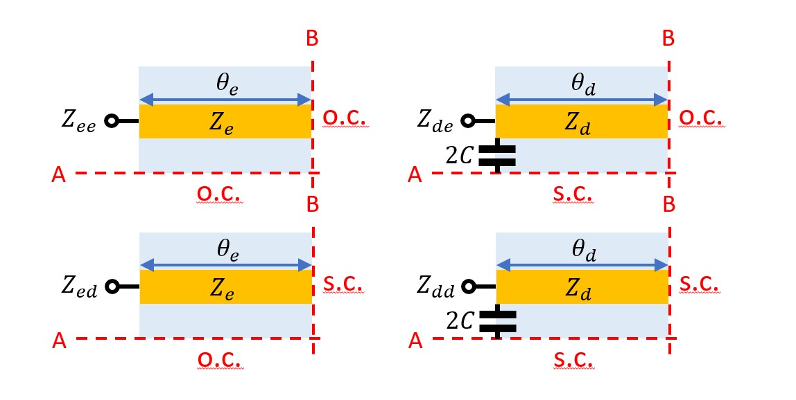 Figure 2. Decomposition of the two-fold symmetrical four-port into four one-ports terminated by o.c. and s.c. within the symmetry planes.
Analysis of Compensated Coupled Microstrip Lines
Figure 1 shows two microstrip lines, which are coupled through the length The feedlines at all four ports are considered to be uncoupled and having the system’s characteristic impedance
 . At both ends of the coupled line section, the lines are connected via two capacitors having the capacitance
 Each of those can be split up into two capacitors of
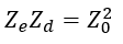
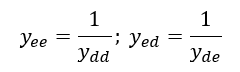
 connected in series. The circuit is considered lossless and perfectly two-fold symmetric with the symmetry planes A and B. It can be easily observed that the capacitors are, with respect to symmetry plane A, only effective for the odd-mode. Otherwise, one of the capacitor's terminals is connected to the virtual open circuit in even mode. The relation between even-mode impedanceodd-mode impedanceand the system’s impedanceis defined as:
(1)
The characteristic impedances of the coupled transmission lines can be normalized as follows:
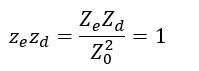
(2)
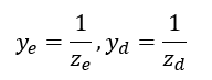
The normalized characteristic admittances of the even- and odd-mode can be calculated by inversion of the impedances:
 (3)
(3)
The two-fold symmetrical four-port can be decomposed into four one-ports10,11, as depicted in Figure 2. These four one-ports are terminated by different combinations of o.c.and s.c. within the symmetry planes. Alternatively, o.c. and s.c. are often called magnetic and electric walls, respectively. The corresponding normalized eigenadmittances of the network can be calculated by transmission line theory:
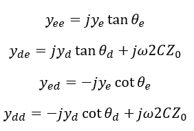
(4-7)
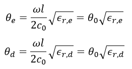
The first and second index denote the mode with respect to symmetry plane A and B, respectively. The electrical length of the even and odd-mode is referred to as and
and  The eigenreflections, then, can be calculated according to:
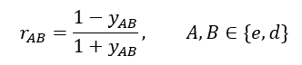
(8)
Scattering parameters can be easily calculated as they are linear combinations of the eigenreflections:
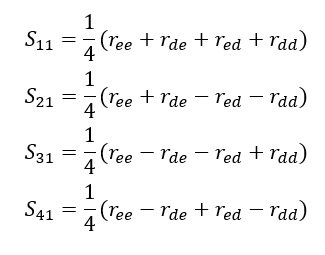
(9, 10, 11, 12)
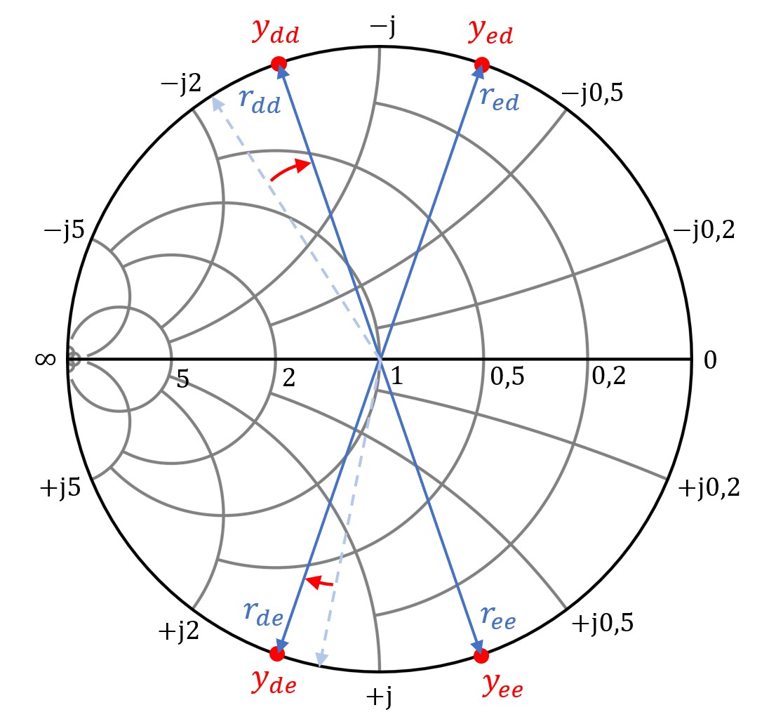 Figure 3. Typical constellation of eigenreflections (dashed: uncompensated, solid: compensated) in the admittance smith chart for a single frequency.
A typical constellation of eigenreflections for two coupled microstrip lines with is shown in Figure 3. The uncompensated eigenreflections are represented by the dashed arrows, while the compensated are represented by the solid arrows. The effect of the capacitors can be regarded as an extension of the electrical lengthThus, the eigenreflections
 and
and  are rotated clockwise, which is indicated by the red arrows. Note that Figure 3 represents the principle of compensation, but a perfect compensation by two capacitors as shown is not possible forandsimultaneously when. This will become clear by the equations presented below.
As the FEXT shall be minimized, the desired scattering parameter is zero. From Equation 11 and the assumed constellation of eigenreflections in Figure 3, two criteria for= 0 can be derived by what is essentially complex vector addition:
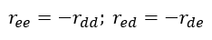
(13)
These two criteria must be fulfilled at the same time in order to forceto be zero. As a 180-degree phase shift of a reflection coefficient is equal to the inversion of the corresponding impedance or admittance, the two criteria can be written as:
(14)
By inserting the Equations 4-7 into Equation 14 and solving for the capacitance value, the two competing results can be obtained:
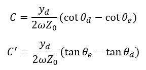
(15, 16)
With the help of common trigonometric addition formulas, Equations 15 and 16 can be written as:
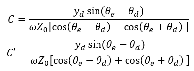
(17, 18)
It can be seen that when
when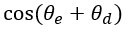 = 0. Therefore, the argument of the cosine function has to be:
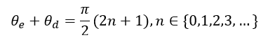
(19)
The electrical lengthand can be expressed as
(20, 21)
with the angular frequency and the speed of light
 . By inserting Equations 20 and 21 into Equation 19, the “free-space,” electrical length can be calculated as:
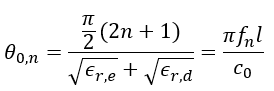
(22)
Therefore, perfect isolation is possible for the
 single frequency points:
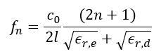
(23)
When assuming thatthe Equations 17 and 18 become identical and Equations 20-22 can be inserted. Therefore, the choice of the following capacitances values leads to perfect isolation:
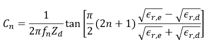
(24)
For Equations 23 and 24 simplify to:
(25, 26)
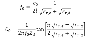
Equation (25) presents the relation between the length of the coupled line structure and the frequency where perfect isolation can be achieved when compensation capacitances as calculated in (26) are used. For small arguments of the tangent-function, i.e. small differences betweenand, the equation (26) can be approximated by:
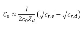
(27)
This approximation may be sufficient in many cases, however, in the following the exact solution according to equation (25) and (26) is used. The example in the next section shows that improvement of isolation is not only obtained for the frequency but for a wide bandwidth around that frequency.
Example
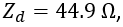
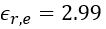
Let’s assume an example with two microstrip lines of width 1.73 mm with 1 mm space between them on a Rogers RO4003C high frequency laminate, having a dielectric permittivity of 3.55 and a substrate height of 32 mils (which equals 0.813 mm). The length of the coupled section shall be 50 mm. The even and odd parameters are approximately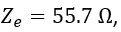
 and
and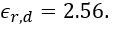 With Equations 25 and 26, perfect isolation is achieved at a frequency
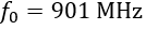 for a capacitor of
 Figure 4 shows calculated scattering parameters for the uncompensated and compensated coupled microstrip lines. It can be observed that for the compensated case, the isolation improves considerably over the whole frequency range whilst the matching worsens and the coupling to port 4 increases with frequency. In order to achieve a better performance at higher frequencies, the 50 mm line can be split up into segments, for example, each 10 mm long. Every 10 mm section is compensated perfectly at
 using a capacitance of
 according to Equations 25 and 26. Figure 5 shows the circuit topology. Simulation results are depicted in Figure 6. It can be observed that the isolation performance has improved over a wide frequency range while proper matching and low backwards coupling (equivalent to near end cross-talk, NEXT) are maintained. It should be noted that the approximation in equation (27) leads to essentially the same results, as the capacitance values differ only around 0.12% with respect to the ideal results of Equations 25 and 26. Time domain simulations have been carried out using Keysight ADS;, results are shown in Figure 7. A step signal having a rise time of 100 ps excites the circuits while all ports are terminated with the system’s impedance of
 The input signal
 at port 1 is clearly affected by the capacitances. In the case of the two large capacitors, the rise time is slowed down a bit; after around twice the delay time of the transmission line, the reflection from the end of the line can be clearly observed at around 600 ps. Multiple capacitors lead to multiple smaller discontinuities, of which smaller reflections occur. The output signal
 at port 2 exhibits an additional delay of around 11 ps for both compensated networks. The FEXT at port 3 is considerably reduced from more than 100 mV maximum amplitude to around 31 mV for the compensation with two capacitors and 14 mV for the compensation with multiple capacitors. The NEXT at port 4 increases from a maximum amplitude of 54 mV to 107 mV and 75 mV.
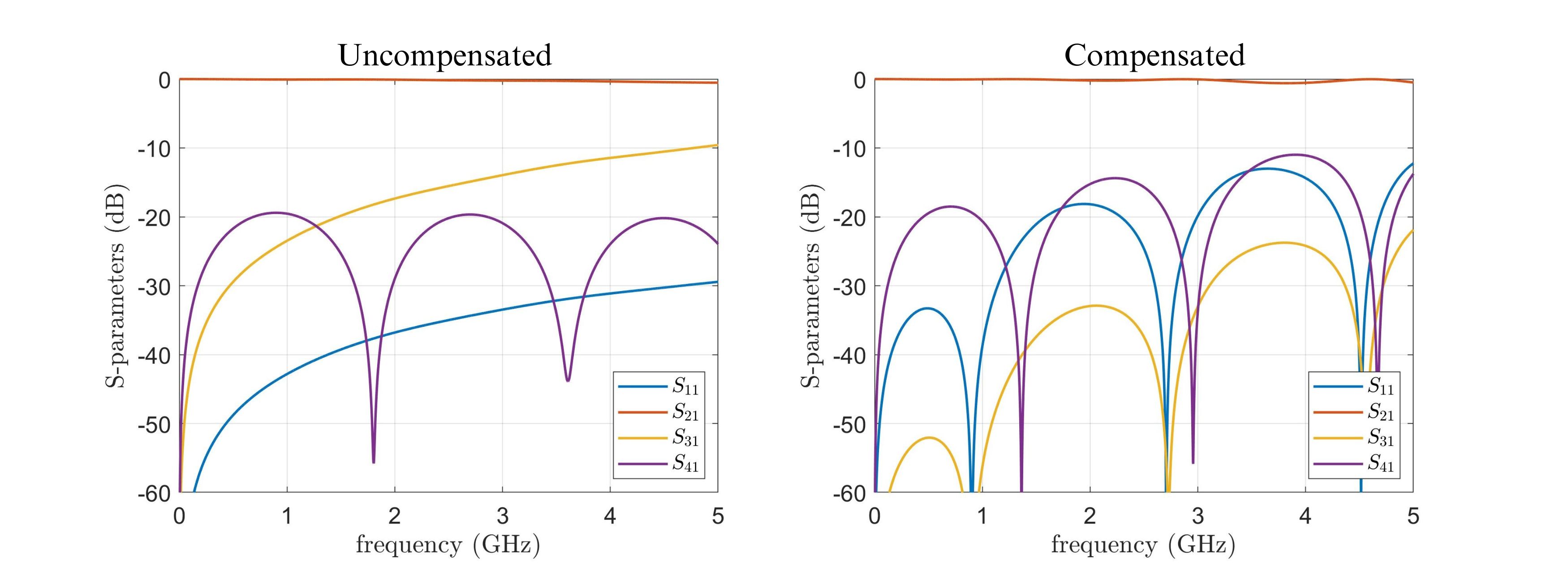 Figure 4. Calculated S-parameters, uncompensated and compensated.
 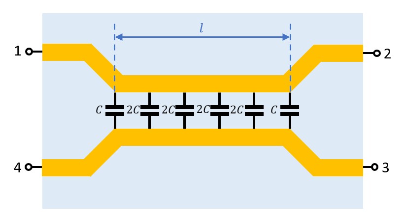 Figure 5. Circuit topology with multiple compensation capacitors.
 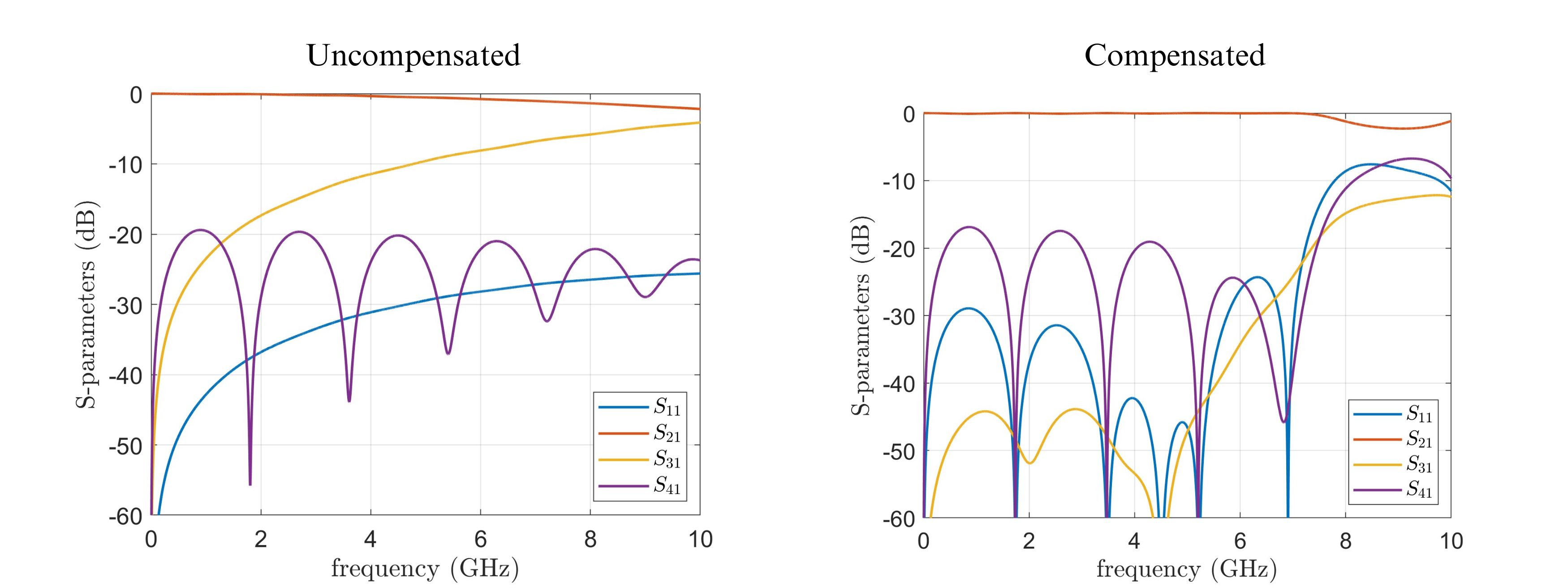 Figure 6. Calculated S-parameters, uncompensated and compensated with multiple capacitors.
 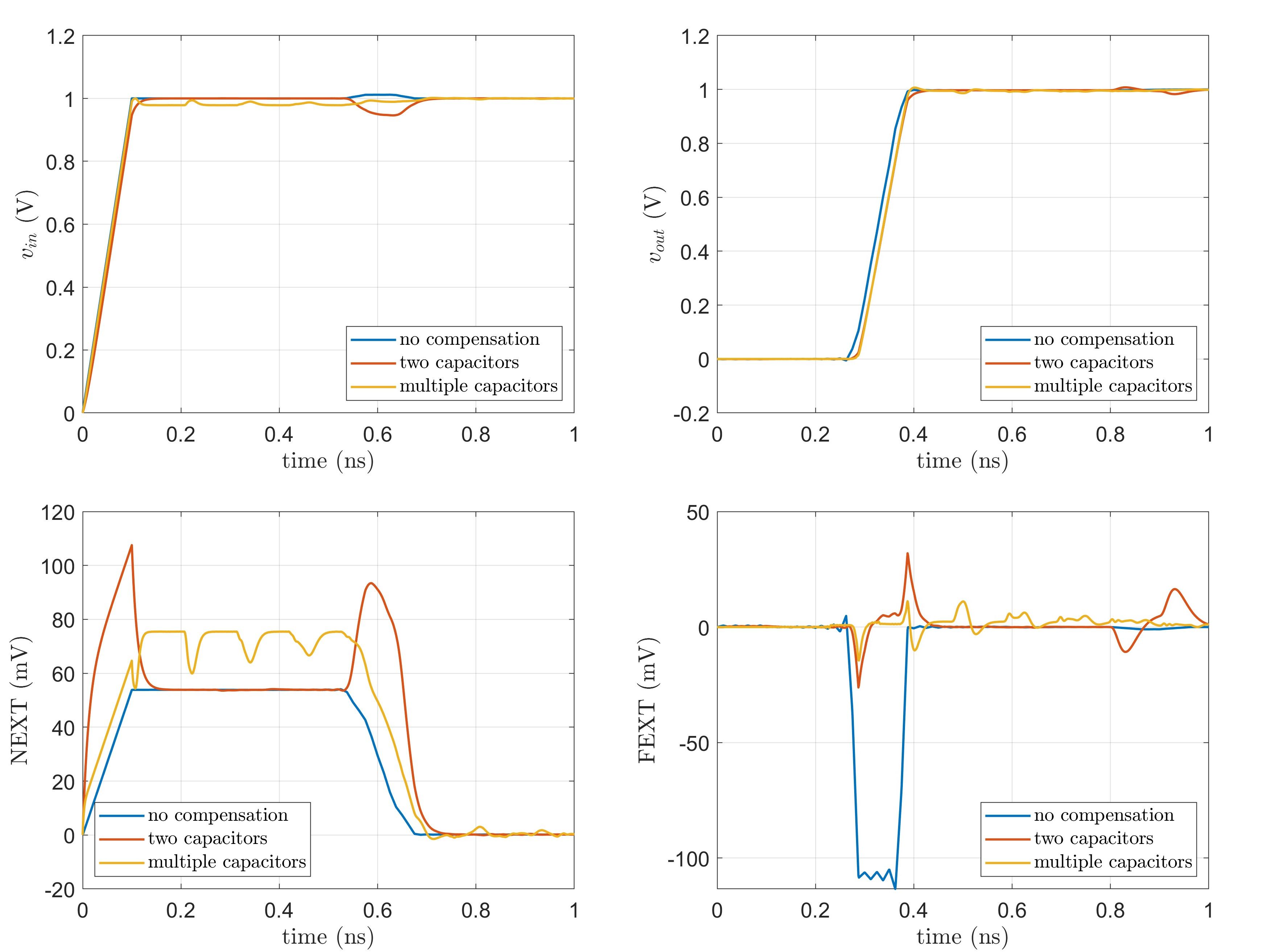 Figure 7. Time-domain simulation results.
 Conclusion
A method for the determination of capacitor values for compensation of unequal phase velocities in coupled microstrip lines has been presented. Simulation results show that broadband performance can be achieved with multiple capacitors along the coupled lines. In practice, the low capacitance values (a couple of femto-Farads) can be realized by stubs, interdigital capacitors, or the modulation of the space between adjacent microstrip lines. The presented equations help to find the maximum allowed distance between the capacitive elements and their required optimum capacitance values. In reality, there are, of course, often more than two transmission lines. Losses have to be considered, as perfect symmetry is not a given and other non-idealities have to be taken into account.
References
1. R. K. Kunze, Y. Chu, Z. Yu, S. K. Chhay, M. Lai, and Y. Zhu, “Crosstalk mitigation and impedance management using tabbed lines,” Intel White Paper, 2015.
2. Wu, C.H., Shen, L., Zhang, H. et al. Equivalent circuit parameters of planar transmission lines with spoof surface plasmon polaritons and its application in high density circuits. Sci Rep 9, 18853 (2019).
3. Q. -M. Cai, Y. Zhu, R. Zhang, Y. Ren, X. Ye and J. Fan, "A Study of Coverlay Coated Microstrip Lines for Crosstalk Reduction in DDR5," 2020 IEEE International Symposium on Electromagnetic Compatibility & Signal/Power Integrity (EMCSI), Reno, NV, USA, 2020, pp. 581-585.
4. A. Podell, "A high-directivity microstrip coupler technique," 1970 IEEE MTT-S Int. Microwave Symp. Dig., pp. 33-36, 1970.
5. G. Haupt and H. Delfs, “High-directivity microstrip directional couplers,” Electron. Lett., vol. 10, pp. 142–143, May 1974.
6. Broadband directional couplers using microstrip with dielectric overlays," IEEE Trans. Microwave Theory and Tech., vol. MTT-22, pp. 1216-1220, Dec. 1974.
7. G. Schaller, “Optimization of microstrip directional couplers with lumped capacitors,” Int. J. Electron. Commun. (AEÜ), vol. 31, pp. 301–307, 1977.
8. M. Dydyk, “Accurate design of microstrip directional couplers with capacitive compensation,“ IEEE MTT-S Symp. Dig., pp.581-584, 1990.
9. C. T. Nghe, F. Rautschke and G. Boeck, "Performance optimization of capacitively compensated directional couplers," 2017 47th European Microwave Conference (EuMC), Nuremberg, Germany, 2017, pp. 408-411.
10. C. G. Montgomery, R. H. Dicke, and E. M. Purcell, Principles of Microwave Circuits. New York, NY, USA: McGraw-Hill, 1948.
11. H. Mextorf and R. Knöchel, "The Intrinsic Impedance and Its Application to Backward and Forward Coupled-Line Couplers," in IEEE Transactions on Microwave Theory and Techniques, vol. 62, no. 2, pp. 224-233, Feb. 2014.