
Power Integrity (PI) engineers are familiar with the ground shield effect in the 2-port shunt through measurement. If not, there are many papers, articles, and videos on the subject.1,2 PI engineers are less knowledgeable about the impacts on other power related measurements. In this article, we focus on power supply rejection ratio (PSRR), power supply modulation ratio (PSMR), and power supply noise rejection (PSNR) measurements, which are all measures of how power rail noise appears at the output of voltage regulators, RF amplifiers, and digital channel jitter.3
 A more accurate representation includes the interconnecting cables as shown in Figure 2. This setup is showing just the modulation signal, as seen at the 1 Ohm load. Note that the benchtop power supply voltage had to be increased by 640 mV to account for the cable voltage drops in order to produce 3.3 V at the output side. This schematic includes 1 m cables, though this is a somewhat arbitrary choice, as is the selection of the cable connector type.

The modulated signal at the load resistor is shown both with and without the interconnecting cables in Figure 3. There are four interesting observations in the resulting simulations. First, the addition of the cables attenuated the modulation signal by about 9%. Second, the bandwidth of the modulated signal is reduced by 42%. Third, both modulation signals are significantly attenuated by several MHz. Finally, the addition of the cables introduced a sharp resonance just above 10 MHz. 
The impedance of the modulation signal at the load resistor is also simulated for these two cases—with and without the interconnecting cables. The impedance results are shown in Figure 4. The interconnecting cables more than doubled the inductance of the interconnect as seen at the load. 
Why This Matters
New, higher speed devices require testing to much higher bandwidths than the results of either of these simulations. Consider the new QSFP-DD Rev 6.2 PSNR requirement for the QSFP Double Density 8× and QSFP 4× pluggable transceivers. A summary of the modulation requirements is shown in Table 1.

This new specification requires a signal injection of up to 10 MHz, while some PLL applications require modulation signals of up to 50 MHz.
Consider the QSFP-DD Class 7 Requirement, which defines the power rail voltage as 3.3 V and the operating current as 5.6 Amps. The equivalent load resistance is: 
The 3 dB modulation bandwidth impact, due to the interconnect, is defined by the frequency at which the interconnect impedance is equal to the load impedance: 
Where L is the interconnecting inductance of the power rail seen at the load. Solving for the allowable interconnect inductance 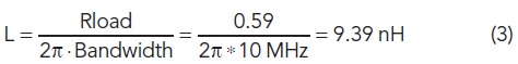
The required interconnect inductance is much lower than the Picotest J2120A line injector can provide, even without the cables included. The addition of the cables exacerbates the situation.
Parallel wires, close together, result in an inductance of about 10 nH/inch.4 This is shown in Figure 5. Achieving a 9.4 nH interconnecting inductance, assuming the modulator itself introduces near-zero inductance, requires that the modulation signal be less than 1 in. from the transceiver being tested. A passive line injector with a voltage drop of approximately 2 V, and an operating current of 5.6 Amps, dissipates a power of 11.2 W. The line injector itself also needs to offer a bandwidth greater than 10 MHz. Together these requirements present a significant challenge. 
Creating a Solution
Achieving the bandwidth is made possible by utilizing small eGaN semiconductor devices in place of Si. These very small eGaN devices are extremely fast due to very low junction capacitance combined with very low internal resistance.
Reducing the device size along with some other design changes allows the circuit to be miniaturized to the point that the line injector form factor can be a very small form factor probe.
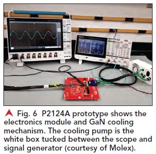
Dealing with the thermal issues is the most challenging task. Placing the device in a small probe allows the line injector to get very close to the device under test. The small form factor also prohibits the use of passive cooling solutions, which would be quite large. The thermal issue is resolved using a very small, precision micro-machined liquid cooling system (see Figure 6).
 The modulation bandwidth required by the QSFP-DD Rev 6.2 specification is 66 mV rms from 40 Hz to 10 MHz. The 3 dB frequencies are shown in Figure 7, with a lower frequency point at 35 Hz and an upper frequency point at 40 MHz. Two points are added at 10 and 100 kHz to show the midband flatness.
 Though the signal is attenuated at higher frequencies by the interconnect wire inductance and the transceiver resistance, it is possible to modulate at 250 MHz, or higher, as shown in Figure 8.
-
S. Sandler, “How To Test PSRR, PSNR, and PSMR for Sensitive Applications,Including Optical Transceivers”, EDI CON 2022, October 5, 2022.
-
“Ultra-low Impedance (20 micro ohm) Measurement using 2-Port Shunt-Through” – Picotest, 2019.
- S. Sandler, “Cable Shield Resistance Issue in a 2-port Impedance Measurement”, Signal Integrity Journal, Web: https://www.signalintegrityjournal.com/ blogs/15-extreme-measurements/post/2306-cable-shield-resistance-issuein-a-2-port-impedance-measurement.
- “How to Measure Ultralow Impedance (100uOhm and lower) PDNs”, EDICON University, 2018.
- Parallel Wire Inductance Calculator, Web, https://www.allaboutcircuits.com/ tools/parallel-wire-inductance-calculator/.