
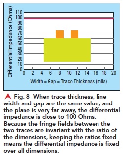
This is a remarkable observation and is the origin of another simple rule of thumb: for traces with an aspect ratio of 1, and a trace width equaling gap separation, the differential impedance of a pair is 100 ohms when the return plane is very far away, and the pair is effectively sitting on a dielectric slab with a dielectric constant of 4.
It is a convenient coincidence that this aspect ratio of 1 for conductor thickness and gap separation contributes just the right amount of fringe fields to bring the differential impedance to 100 ohms without the need for an adjacent return plane. This is an easy rule of thumb to remember and offers a simple anchor point from which to scale other conditions.
For example, for a thinner conductor, the differential impedance will go up. For a larger gap separation, the differential impedance will go up. For a narrower line width, the differential impedance will go up. For an aspect ratio greater than 1, the gap separation would have to increase to maintain 100 ohm differential impedance.
This rule of thumb applies to any pair with any linewidth having an aspect ratio of 1. However, since conductor thicknesses in conventional circuit boards are on the order of 0.2 to 3 mils, this rule of thumb really applies specifically to ultra-fine line geometries, with line widths less than 3 mils.
When the aspect ratio is less than 1, the differential impedance is higher than 100 ohms for the special case of the line width equaling gap separation. To achieve a 100 ohm target impedance, the return plane must be moved closer to the pair to increase the coupling of the two lines. This defines the design space for 100 ohm differential pairs, and is shown in Figure 9.

This map of design space for a 100 ohm differential pair clearly shows the new emergent behavior starting when the aspect ratio is greater than about 0.5 and the edge to edge fringe field coupling becomes a first order effect. This is the regime of ultra-fine line geometries.
There are two important consequences from this behavior. First, it is possible to achieve a 100 ohm target impedance when the return plane is moved farther away than the span of the differential pair. This means that when ultra-fine line technology is mixed on the same layer as conventional line width technology, the 100 ohm differential impedance can easily be matched using appropriate line width and gap separation.
The second consequence is that for an aspect ratio of conductor thickness to line width larger than 1, the gap separation will generally have to be larger than the line width to hit a 100 ohm target impedance. Higher aspect ratio geometries will require a ratio of less than one line width to the gap separation.
The regime of ultra-fine lines, with aspect ratios of trace thickness to line widths greater than 0.5, requires a re-calibration of our design intuition to include the first order effect of the edge-to-edge coupling, without the need for an adjacent return plane. These are important considerations when mixing ultra-fine line and conventional circuit board technologies.
For example, for 1 oz copper traces, when the line width is 5 mils and the gap separation is 5 mils, the dielectric height to the adjacent plane would have to be 4 mils to achieve a target impedance of 100 ohms. Any other pairs sharing this layer with a span of less than 4 mils would have a differential impedance independent of the adjacent plane. This is a new design regime which specially applies to ultra-fine line geometries.
Design Space for Ultra-Fine Lines with No Return Plane
When mixing conventional and ultra-fine line geometries on the same layer, the ultra-fine line differential pairs routed with their smallest span will generally not couple to the adjacent plane. Our design intuition in this regime is very different than when the adjacent plane influences the differential impedance.
In the special case of differential pairs with their dielectric thickness to the return plane farther away than their span, their differential impedance is only about their line width, gap separation, and conductor thickness. As we would expect, the differential impedance is more sensitive to the gap separation than the line width.
Of course, for a fixed gap separation, as the line width increases the differential impedance will decrease, but it is only slowly varying with line width. The faraway edges of each line do not couple as strongly as the adjacent edges of the two traces that make up the differential pair.
However, the differential impedance is strongly dependent on the gap separation, as this is the region where most of the coupling between the two traces occurs. Thismeans that for a fixed line width, the differential impedance will change rapidly with the gap, but not so rapidly with line width.
In each case, the differential impedance will decrease for thicker conductor due to the additional fringe field coupling from the relatively larger side walls.
These two general trends, with a return plane very far away, are shown in Figure 10 for up to a 10 mil span dimension. In one case, the line width is fixed at 2 mil and the gap separation is increased, and in the other case the gap separation is fixed at 2 mils and the line width of each line is increased. In all cases, the dielectric thickness is adjusted so that it is always larger than 3x the span, effectively infinitely far away.
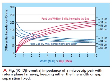
This analysis shows that in this regime where the return plane plays no role, the gap separation has a stronger impact on the differential impedance than the line width.
We can use the Johnny Cash Principle, introduced in Part 2, to define design space for a 100 ohm differential pair as its span changes. At each value of the span, there is one unique value of line width and gap separation that results in 100 ohm differential impedance.
This 100 ohm design space is shown in Figure 11, using the special case of 1 oz copper traces, all with the coupling between the two lines much larger than the coupling to any distant plane.

For example, in the case of 1 oz copper for a 100 ohm target impedance when the span is on the order of 4 mils, the gap will be about 1.3 mils and the line width will be about 1.3 mils.
Mixing Conventional and Ultra-Fine Line Technology
One strategy for mixing conventional and ultra-fine line traces on the same layer is to use as wide a trace as is practical for its lower conductor loss, and only use the ultra-fine lines where the higher interconnect density is needed for routing in congested breakout regions.
If the top layer microstrip traces are designed with ¼ oz copper and a 5 mil wide line and 5 mil space differential pairs, a 100 ohm differential impedance will be achieved with about a 4 mil thick dielectric to the adjacent plane. Any pair with a span smaller than 4 mils will not be influenced by the adjacent plane.
On this same layer, if ultra-fine lines were used, with a conductor thickness of 6 u (1/4 oz copper), line widths of 6 u, and a gap of 6 u, their differential impedance would be 100 ohms. These dimensions would enable four routing tracks between 0.5 mm BGA pads. These high-density tracks could be used to fan out from the BGA escape to a coarser routing field. Figure 12 illustrates two different transitions from the ultra-fine line to the coarser traces while maintaining 100 ohms differential impedance.
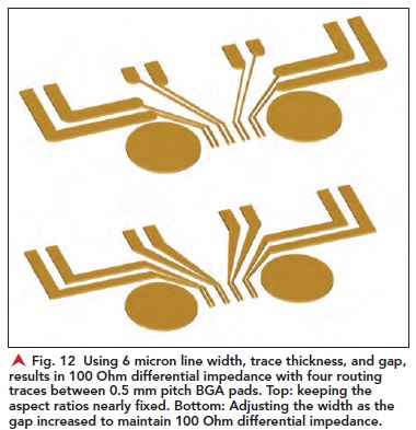
If the transition region is short, even if the differential impedance is not held constant, the impact from this discontinuity may be acceptable. This mixed line width approach optimizes the interconnect density where needed and the lower loss from wider traces where it is available, while maintaining a constant 100 ohm differential impedance.
Conclusion
With the recent introduction of ultra-fine line fabrication technologies, it is possible to mix very fine line traces with conventional circuit board traces on the same layer. This provides the advantage of using ultra-fine lines for regions of congested routing while wider traces can be used for longer paths where reducing signal loss is important.
However, when these very different trace widths are routed on the same layers, and the differential impedance of pairs are kept at 100 ohms, new design guidelines emerge for the ultra-fine line traces due to two important emergent behaviors.
First, when their span is less than the dielectric height to the adjacent plane, the plane has no influence on the differential impedance. It is just about the line width, gap separation, and conductor thickness; there is one unique combination of line width and gap separation for a specific span. This defines the design space for these traces.
The second important design consideration is that in this regime of very fine lines, the aspect ratio of conductor thickness to trace width increases over conventional technology, and the side wall coupling between the two traces becomes a first order effect. This new coupling must be taken into account when designing the differential pair.
In the extreme case, with no adjacent return plane, a differential pair with trace thickness, line width, and gap separation all of the same order will result in a 100 ohm differential impedance.