
The temperature difference tends to be smallest for widest traces, and it increases as pad/trace width narrows. Nevertheless, spot temperatures under even the narrowest traces are still significant. Not discussed here (see again, [3]), temperature differences are a function of board thickness. Temperature differences will increase as the board thickness increases.
The results tend to confirm the general statement above: the thermal profile of the bottom layer of a circuit board resembles the thermal profile of the top layer. The difference in spot temperatures is typically less than 10 oC between the top and bottom layers and is more often in the range of 5 oC or even less.
Implications
There are several possible implications to the above. First, these results explain why thermal vias are so inefficient, they are almost ineffective. Thermal vias, by definition, have to go somewhere. Typically, they terminate on a copper surface (plane) on the opposite side of the board. Equation 1 shows the theory behind them. The formula for thermal conduction is:
Equation 1. Q/t = kA(ΔT)/d
Where:
Q/t = rate of heat transfer (watts, or joule/sec)
k = thermal conductivity coefficient (W/m·K)
ΔT = change in temperature (oC = oK)
A = Overlapping area
d = distance between pad and plane
In the example above (Figures 2 and 3), the heated pad (without an underlying plane) is 73 oC above ambient (ΔT=73). But in this case, there is no place to terminate a thermal via. When we add a plane on the bottom layer, something to which we can terminate the thermal via, the ΔT (between pad and plane) lowers to 9 oC. (The internal plane case lowers the ΔT to 6 oC.) Almost all the benefit comes from the addition of the copper plane itself. The marginal contribution of an additional thermal via is almost negligible.
A second implication is that smaller signal traces on inner layers will have nearly the same thermal profiles as the top and bottom layers above and below them. Figure 6(b) illustrates an inner trace layer, about 6 mils below the top layer, passing underneath one of our heated pads (no plane underneath). There are two traces, 1.0 mm and 2.0 mm (40 and 80 mil) wide, respectively, passing underneath the pad. Figure 6(a) is the same pad without any traces.
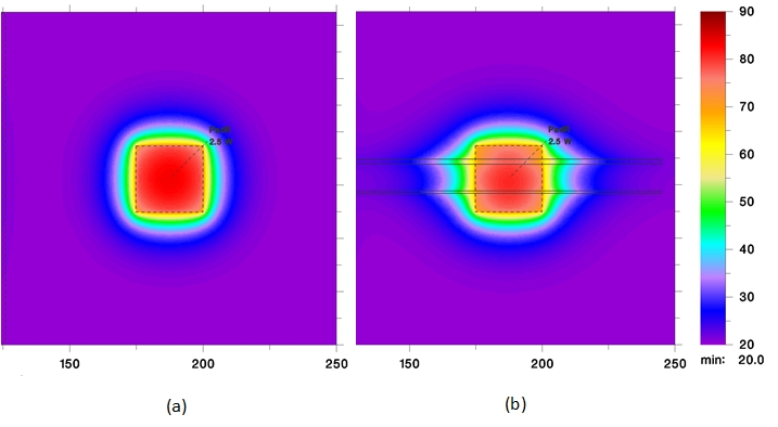
Figure 6. Comparing the thermal patterns underneath a heated pad with no internal traces (a) and internal traces 6 mils underneath the pad (b).
The thermal pattern illustrates that the traces influence the cooling slightly (smaller traces would have a smaller impact), but overall, the signal traces have almost the same thermal profile as the heated pad. Since resistivity is a function of temperature, this means that the resistance of the signal traces changes from point to point along the trace as it passes underneath the pad [4]. One can speculate that this means that the resistance of each side of a differential pair, or the resistance of different differential pairs in a signal bus, might be different if they pass through different thermal environments. This may or may not have an impact on signal levels and timing, depending on circumstances.
Experimental Evidence
An appropriate question is: do we have any experimental evidence to support the type of thermal profiles we talk about herein? The answer is yes. For example, in a recent article [5] we showed (experimentally) that a trace routed underneath a pad changed resistance if the pad changed temperature. We then asked if this had any signal integrity implications.
In our book [1] we devote Chapter 8 to via heating. In that chapter we have two tables that confirm our simulation models match our experimental test board [6]. Figures 7 and 8 are adapted from Figures 8.8 and 8.9 in that chapter. These thermographs are from experimental six-inch long traces with a via in the middle, going from the top to the bottom layer. The left-hand portion of each trace is on the top layer. The left-hand temperature indications are for the trace/via on that top layer. The right-hand portion of each image is the temperature on the top layer heated from the actual trace on the bottom layer.
In Figure 7, the right-hand top layer is about 10 degrees cooler than the equivalent spot on the opposite layer. But in Figure 8 the difference is only about one to two degrees cooler than the opposite layer. This is consistent with our simulations above. The temperature difference reduces as the heated width increases.

Figure 7. 27-mil wide trace carrying 6.65 Amps (adapted from [1], Figure 8.8.)
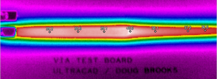
Figure 8. 200-mil wide trace carrying 8.55 Amps (adapted from reference 1, Figure 8.9).
Bottom Line
The thermal impacts of heated traces and pads are not limited to the board layer on which they exist. They are reflected, to a greater or lesser extent, on every layer above and below them.
Notes