
In my consulting work, I have noticed that radiated emission (RE) and radiated immunity (RI) have become much more pervasive issues for most of my clients. There are several reasons for this, which include the shift to more compact design, more portable products, as well as the fact that noise margins for digital logic levels continue to be reduced as supply voltage decreases (The popularity of using ARM based architecture means 3.3V systems replace 5V systems).
The root causes for failing RE and RI could be a bad layout design, an unshielded noisy node, noise coupling cables, etc. Among them, a high percentage of failures are related to structure resonances in a system. Structure resonances could be in large systems where two systems joined with cables, or a small daughter board that is mounted on the main PCB. In most cases, structure resonances cause radiated emission failures at their resonant frequency, they also fail radiated immunity tests at the same frequency range thanks to reciprocity. (Reciprocity means that if a structure radiates well, then it will also pick up energy well, and vice versa [1].)
A tremendous amount of work has been done on this subject previously. In [2], plane and cavity resonances were demonstrated and practical examples were given to show the physics behind resonances. [3] covers the transmission line theory behind resonances and various examples were given to illustrate the point. Smith’s website [4] has more than 10 short articles (what he calls Technical Tidbits) covering resonance structures, mostly to do with measurement techniques using magnetic field loops. Other ways of measuring resonances include using a spectrum analyzer and an antenna [5]. Methods of fixing resonances are also included in [1]- [5].
The most effective methods of fixing resonances are damping (by using multiple connections or resistive connections), the ferrite approach (again, using the resistive part of the ferrite rather than the inductive part as a pure inductor generates reflection), applying EMC shielding (depends on the ground structure, as we will discuss later), or simply re-designing (often easier said than done).
This article presents some case studies in the field; I have tried all the methods introduced in the literal review and use the most cost-effective (both in financial terms and time frame) method to identify and locate the resonance structure. Fixing the issue depends on the product design, as there are often many constraints. The most cost-effective way of fixing the problem comes with relentlessly trying different approaches.
Case study 1 – Radiated emission associated with MOSFETs
Identify the resonant structure
A DC-DC converter experienced both conducted and radiated emissions during the EMC tests. Since it is a switched mode power supply (SMPS), experience tells us the switch node (which is associated with the switching devices and the layout) is often the culprit. The switching devices used in this product are MOSFETs in a TO-247 package.
The benefits of using surface mounted switches over through-hole devices from the EMC perspective were covered in [6]. Basically, the long leads of a TO-247 package introduce about 10nH inductance, together with the self-capacitance of the MOSFET (estimated to be 4nF in this case), so an L-C tank circuit is formed. The ringing observed during a switching event has shown a 20MHz resonant frequency, and it aligns well with the failures observed in the conducted emission test.
The unit also failed radiated emission tests at 250 and 360MHz. A visual inspection on the MOSFET layout (see Figure 1) shows that the PCB has a cut-out area the same size as the MOSFET cooling pad, so that the MOSFET can be mounted to a heatsink via the screw connection through the PCB cut-out areas. (This is a mechanical team’s dream, but an EMC nightmare). Another “interesting” feature of this design is that the MOSFETs and the PCB cut-out areas are all located on the edge of the PCB, so they could radiate very efficiently. This structure could easily resonate as we expected.
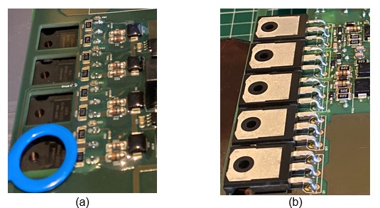 Figure 1: MOSFETs on the edge of the PCB where cut-out areas are designed to allow screws to mount the MOSFETs on heatsink (a) front view (b) back view
Ways to see it
Among the techniques that could be used to measure the structure resonances, the method introduced in [7] is perhaps the easiest and cheapest set-up. A network analyzer or a spectrum analyzer with a tracking generator can do the job. A directional coupler (such as a Mini-Circuits ZFDC-20-5+ or ZFDC-10-5+) is needed to work with a spectrum analyzer, whereas a network analyzer eliminates the need of a directional coupler (since it can determine return loss).
The basic idea is that a small loop radiates RF energy depending on its loop area. Since the area in this case is small, it will only radiate efficiently above 3 GHz or so. Below this frequency, most of the RF energy bounces back due to reflection. The directional coupler directs some of the reflected energy, so one expects to see a flat curve on the tracking generator result. If the loop is close to a resonant structure, however, the RF energy could be absorbed by that resonance structure, causing a dip in the spectrum analyzer tracking generation plot results. See a video demonstration of this in [8].
Figure 2 shows the test set-up (with spectrum analyzer, directional coupler, and a shielded magnetic loop). A shielded loop is supposed to perform better for this kind of test as it avoids capacitive coupling of the loop itself. But, in reality, both shielded and non-shielded loops prove to work equally well most of the time.
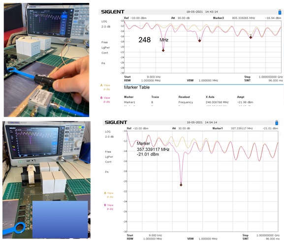 Figure 2: Use the technique introduced in [7] [8], resonance point can be easily seen in the spectrum analyzer tracking generator result. In this case, both resonant points that failed the radiated emission test were located.
The Fix
Since the issue was identified in a late stage and the system under test is rather large (as the PCB is only a part of the system), a re-design of the PCB is impossible. There are, however, two cost-effective ways of reducing the impact of the resonance.
- Putting a small lossy square-loop ring core on the transistor leg is often good for this sort of problem. This is a technology that was used in the 1990s, but it still finds its way into today’s designs: see Figure 3(a). The core increases inductance, but the ring is damped. Therefore, the frequency and amplitude of the resonance go down. Also, the square loop material delays the current rise, making the switching softer.
- Inserting an EMI flexible absorber sheet between the devices and the PCB can help. Modern absorber sheets often have a high permeability and can serve as a good thermal conduction material, so they are perfect for this application.
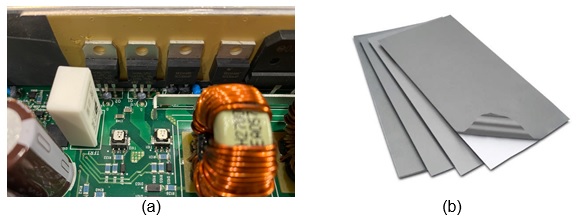 Figure 3 (a) small lossy ring core on the drain lead of through hole devices (b) flexible EMI absorber sheets sometimes also have good thermal conductivity
Case study 2 – Radiated immunity caused by replacement of an IC
Retrofitting a new IC to replace an older technology in an existing product often is not as easy as it sounds. Problems such as failing to function reliably or causing EMI issues could occur. Often such a fault is discovered after the original IC is no longer available in the market.
In the following example, a company is caught by surprise when they found a new IC daughter board they designed and mounted on the original IC pinout location has suffered from radiated immunity issues. Since the product is a sound product, tone issues were found when the unit was exposed to radiated emissions around 1.2GHz to 1.4GHz. The original IC is no longer available after more than 10 years of service time. The new IC is based on ARM architecture and is powered by 3.3V.
Identify the resonant structure
Both the original IC and the small daughter board that replaces it are shown in Figure 4 (a) and (b), respectively. The backside of the daughter board shows that the pin legs are also bent 90 degrees on the connection points, which inevitably introduces inductance in the connection between the two boards.
The daughterboard (with circa 374 mm2 area, 5 mm distance to the main board) forms a capacitance of approximately 1 pF (based on the simple equation C=ε0εRA/h). The long trace from the daughter board to the main board can easily have a 10nH inductance. The self-resonance of this board is then estimated to be 1.5GHz, indicating the system is more likely to have immunity issues at this frequency range.
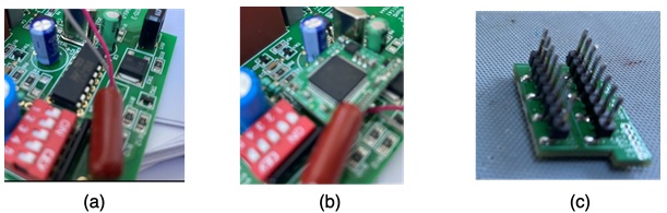 Figure 4 (a) original IC (b) the new daughter board (c) the pin legs on the backside of the daughter board
Measurement
The same method as the previous case study could be used to identify/locate the structure resonance. As one probes the field probe around the daughter board, dips in the tracking generator results can be seen in the frequency range that causes immunity issues (see Figure 5).
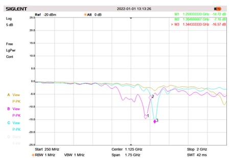 Figure 5 Resonant points identified
Alternatively, if a spectrum analyzer is unavailable, one can use a signal source that is capable of producing the signals in the frequency range of interest (in this case frequencies up to 2.1GHz) and a high bandwidth oscilloscope (at least 1GHz in this case), together with two square magnetic field loops. The set-up is shown in Figure 6, where one magnetic loop is used to generate noise across a wide frequency on the daughter board, and the other magnetic loop is placed alongside the 0V trace on the mainboard. When the RF noise hits the resonant frequency, one can see a sudden jump in amplitude of signals measured in the oscilloscope. The jump in amplitude indicates at resonant frequency, the ‘ground bounce’ between the two boards becomes more obvious. The magnetic field loop basically picks up the noise via mutual inductive coupling between the trace and one side of the loop. One caution in using this method is to be aware of the close field coupling between the two magnetic field probes.
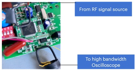 Figure 6 Another set-up using two magnetic field probes, an RF source and high bandwidth oscilloscope
Problems, Challenges and Fix
One of the issues with the structure resonance in an immunity test is that once the RF energy is absorbed by the structure, RF current starts to flow on the traces of the PCBs. One particular issue is the ‘ground bounce’ caused by common-mode current flowing between the 0V of the daughter board and the main board. In fact, it was believed this was the main issue causing the tone change problem in this product, since the driver stage for the speaker is rather weak and there’s no ground plane on the main board design.
The challenge here is that at such high frequency, measuring the “ground bounce” is extremely difficult, especially if high frequency precision measurement equipment is not available. Trying to measure this using a FET probe might not be good enough as 1pF capacitance (which often comes as the intrinsic capacitance of a FET probe) at 1.3GHz has an impedance of 122 ohm. Using a typical passive probe is a no go, because 10pF (often the intrinsic capacitance of a high impedance passive probe) at 1.3GHz is only 12 ohm. In fact, using a passive probe, even with the shortest lead, provides a perfect path between the two 0V of the boards under test. Therefore, the immunity issue “magically” disappeared, an experience that could be very frustrating for even experienced engineers. This was demonstrated in a video [9].
On the product side, the constraints are:
- The main board was designed many years ago, it is only a 2-layer PCB without ground/power plane. The design cannot be changed for this revision.
- The manufacturers have already manufactured tens of thousands of the daughter boards. Getting rid of them will be costly, also not in good spirit for the environment.
- The options to fix the issue needs to be cost-effective, which is often the requirement for volume manufacturers.
Mitigation methods that were introduced in previously referenced literature were applied on this design. The result and comments are presented in Table 1. None of the methods seemed to work perfectly well, and the methods listed in the table need intensive manual work in the assembly process.
An effective way, as it turned out, was to insert a flexible EMI absorber sheet in between the PCBs (as shown in Figure 7). 16 pins need to be punched in order to insert the daughter board (which some manufactures can do at an additional cost). One might wonder whether simply putting the sheet on top of the daughter board will do the job. The answer is no, as the resonance is really caused between the PCBs. Since there are many absorber sheets around, the selection should focus on the attenuation at the frequency range of interest and depth of these materials (often thicker sheets perform better).
Another approach, which is quite similar to the method discussed above, is to use a connector EMI suppression plate. Fair-Rite happened to have a part with the same pin layout as the original IC (also suitable height). Therefore, it can be considered as an alternative method; two plates are needed to achieve the required attenuation: see Figure 7(c).
Table 1 Some options for fixing the problem
|
Options |
Description |
Results & Comments |
|
Capacitive fencing on the daughter board |
Putting multiple 22pF and 10pF high frequency MLCCs on the daughter board; the idea is to enhance the decoupling |
Didn’t work in this case, as there’s no ground plane on the daughter board. Noise still travels to the pins. |
|
Applying a shield around the daughter board |
Putting a shield and bond it to 0V on the daughter board or on the main board |
Didn’t work, because, neither the daughter board nor the main board has ground/power plane; there’s no “quiet” RF reference for the shield to be connected with. |
|
Damping the resonance by resistive components |
There’s one 0V connection between the two boards; however, there’s another 0V point on the daughter board that could be connected to the main board via a resistor |
A 50 ohm connection was made on the other corner of the daughter board. There’s improvement, but not good enough. A lower resistance value such as 20 ohm might be a better option. |
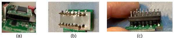 Figure 7 (a) An EMI absorption sheet was inserted between the PCBs (b) zoomed-in view (c) Two EMI suppression plates from Fair-rite were used to achieve the attenuation
Conclusion
This article reviews work on structure resonances and their EMI impact. Methods to identify and locate structure resonances were presented, challenges were discussed, and fixes suggested using practical examples.
References