
Starting at the beginning, the core requirement of an SI engineer is to be able to determine whether a data link has sufficient signal integrity. This typically means evaluating the eye-diagram after equalization to see if there is enough margin to achieve a desired bit-error rate (BER). In order to perform this analysis, an engineer needs accurate models of the channel (transmission lines, vias, and other interconnects), and then accurate models of the transmitter and receiver, known as the IO Buffer circuitry and its packaging. However there-in lies a conundrum. Accurate models of the IO Buffer would lead you to the entire SPICE netlist of the IO Buffer, a level of detail that would contain proprietary information about the IC architecture, would contain 1000s of active transistors, and result in very time-consuming simulations.
The birth of IBIS (I/O Buffer Information Specification)
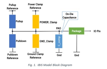
The IBIS was released in 1993 to enable silicon vendors, system EDA tools, and simulation end-users to easily exchange models that would protect intellectual property and simulate faster by providing a model that characterizes the analog performance of the IO Buffer into a transportable file. The equivalent block diagram for IBIS is shown in Fig. 1.
How is the IBIS model characterized?
An IBIS (.ibs) file is a human readable, text-editable file, and it contains multiple sets of measured or simulated table-based data representing how the device behaves. In the case of an output model, the data would contain several lists of supply voltage vs. output current (I-V) data for pullup/pulldown and power/GND clamp. This, together with a simply defined ‘ramp’ slew rate, gives the minimal amount of information a simulator needs. From the I-V tables, the EDA simulator can infer what the current output should be for any channel that we will attach to the output of the IBIS model.
Next, we layer in device behavior for over-voltage and over-current situations. This is done through the Power and Ground Clamp I-V tables, to capture the behavior of the protection diodes found in the IC circuitry. Next, we increase the accuracy of the model with voltage vs. Time (V-T) tables that characterize the exact shape of the rising edges and falling edges as desired (much more detailed information about the waveform than just the slew rate). The V-T tables provide the actual non-linear transition into a known load, which is measured at multiple load conditions.
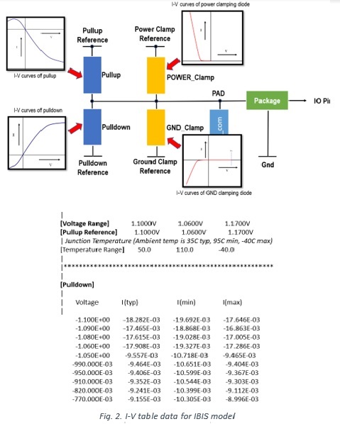
In a nutshell, IBIS models represent I/O buffer behaviors by the table data (I-V, V-T, etc.) from either measurements or simulations, shown in Fig. 2.
Finally, we can layer in information about the package. At its simplest, this is a description of the typical R, L, and C values for the package pins. It can also be expanded to a definition of R, L, and C for each pin individually, as basic transmission line networks, or as RLC matrices, S-parameters or SPICE netlists (the latter two in the very latest version 7.0 of the IBIS Specification, ISS – Interconnect SPICE Subcircuit, to capture coupling between pins).
How does the IBIS model work with EDA tools?
So far, that’s a lot of information to digest, but luckily, usage of a model in the EDA simulator doesn’t need an expert knowledge of how the model was created. Entering keywords, data, and making sure the model is compliant to the standards are all the model developer’s job. The end-users, consumers of the IBIS model, can easily use the model inside an EDA tool. Typically, users only need to point to the IBIS file, then select the right model for their data rate, the right package model to match their use-case, and the model corner to simulate, shown in Fig. 3. Corner? - Yes, there is variability in the how the IO Buffer silicon would perform from one batch of chips to another. To capture this in the model, IBIS files can contain multiple data sets (‘typ’, ‘min’,’max’), for ‘typical, fast, slow, min, max’ variations, as shown in Fig. 2 (b) with an example. An SI engineer is well-advised to run three simulations to check the link performance for typical, fast, and slow model corners to ensure they have enough design margin.

IBIS-AMI (Algorithmic Modeling Interface)
As we have seen so far, IBIS models represent analog electrical behaviors of transmitters and receivers. However, many advanced serializer-deserializer (SERDES) chips employ equalizations such as continuous time linear equalization (CTLE), feed forward equalization (FFE), decision feedback equalization (DFE), automatic gain control (AGC), along with clock and data recovery (CDR) to compensate the channel loss, inter-symbol interference (ISI), and crosstalk. How does IBIS model handle this?
AMI is the modeling interface for SERDES behavioral models that simulate SERDES functionalities such as equalization and CDR. One example of AMI time domain simulation flow is shown in Fig. 4. The AMI flow was added alongside the traditional (SPICE-based) IBIS flow in IBIS version 5.0. The AMI portion is specified in a section of the IBIS file known as the [Algorithmic Model] keyword. The combination of the transmitter’s analog back-end, the serial channel, and the receiver’s analog front-end is assumed to be linear and time invariant.
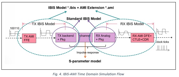
There is no limitation that the equalization should be linear and time invariant in the time domain IBIS-AMI simulation flow. The “analog” portion of the channel is characterized by means of an impulse response leveraging the IBIS constructs for device models. The AMI portion acts as a DSP block which takes an input signal waveform and/or impulse response and outputs a modified waveform and/or impulse response. AMI models are developed by SERDES vendors to match and represent the actual chip behavior. Vendors deliver models in the form of DLL or/and shared object to protect their IP plus the .ami and .ibs text plain files, so that it also provides interoperability between EDA vendors (see Fig. 5).

Advanced AMI models can perform link training communication to tune the transmitter equalizer parameters for optimized performance and adapt to the signature of any analog channel. This is done when transmitter tap parameters are re-configurable and receivers help them to be configured. Advanced communication specifications such as PCI express, USB, Fibre Channel, and IEEE 802.3 define link training protocols for transmitters and receivers.
If both the transmitter and receiver AMI executable models support the same link training protocol (BackChannel Interface Protocol), the EDA tool will facilitate the communication between the executable models, enabling link training. Another name for link training in the industry is AutoNegotiation. A link training algorithm can either emulate what the silicon is doing, or it can use channel analysis methods to determine the optimal Tx equalization settings. This ability will also allow Rx AMI models to determine the Tx equalizations settings for channels that do not have automatic link training capabilities. (1)
For the model developers, the dynamically loaded executable model implements an API (application programming interface) containing up to five functions: AMI_Resolve, AMI_Resolve_Close, AMI_Init, AMI_GetWave, and AMI_Close. The interface to these functions is designed to support three different phases of the simulation processes: initialization, simulation of a segment of time, and termination of simulation. There are comprehensive programming guides in the IBIS specification.
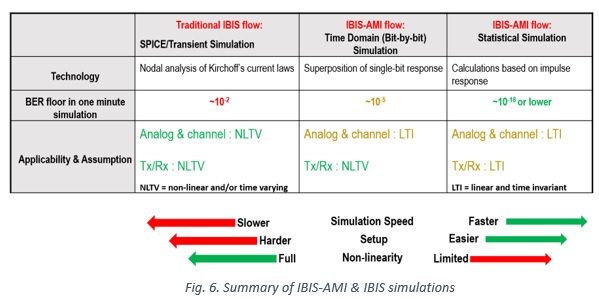
There are two types of simulations that can be performed with IBIS-AMI models, statistical simulation and time domain simulation, which is also called bit-by-bit simulations. If waveform data is needed for data analysis, time domain simulations must be performed. Traditional spice-like simulations, which are also called transient simulations, can handle complete non-linear behaviors of the system. However, the disadvantage of it is the lengthy simulation time, meaning it’s hard to get a good, low-level BER calculations.
For the IBIS-AMI flow, statistical and bit-by-bit simulations assume the analog portion of IBIS model and the channel to be LTI (linear time invariant). The statistical simulation is based on the impulse response of systems, whereas the bit-by-bit simulation adopts the superposition of single bit responses. With these approaches, the simulations can achieve very low BER calculations at very fast simulation time.
By default, every IBIS-AMI model has an AMI_Init function that allows both the statistical and bit-by-bit simulations. However, in this case, the transmitters and receivers are treated as LTI transmitters and receivers. Therefore, non-LTI features like CDR, gain compression, DFE, clock forwarding, etc. cannot be comprehensively handled with AMI_Init. This is where AMI_GetWave function comes in to support those advanced features with IBIS-AMI models. If the GetWave_Exists flag is on, it can handle non-LTI transmitters and receivers. The summary is illustrated in Fig. 6.
For consumers of IBIS-AMI models, there are four cases or scenarios based on what functions are included in the executable model file. AMI_Init and AMI_Close functions are always in the executable model, meaning that both statistical and bit-by-simulations are always applicable. If the non-linear time invariant features are needed, AMI_GetWave must exist and GetWave_Exists flag must be "True" in the IBIS-AMI model, shown in the example in Fig. 7. (Note that AMI_GetWave only works with time domain or bit-by-bit simulations.)

DDR5 and LPDDR5 Applications
As far as applications for IBIS models are concerned, some of the most complex IBIS models have been created for memory interfaces (DDR). This is due to the large number of signal pins, packages, and configurations available (especially thinking about multiple DRAM dice stacked inside a single package of LPDDR4). Up until DDR4/LPDDR4, IBIS models have covered all the simulation needs of the typical SI engineer.
As we move forward to next-generation memories (DDR5/LPDDR5), the technology on chip has evolved, and so must the modeling and simulation technology. In DDR5 and LPDDR5, equalization is available on the commodity DRAM and controller devices for the first time, which came with variable gain, CTLE (continuous time linear equalization), and DFE.
The speed in DDR5 and LPDDR5 systems is increased to up to 6400 MT/s, resulting in worsened ISI impairment. Equalization techniques including deemphasis, CTLE, and DFE are used in memory controller and DRAM to mitigate ISI. Fast speeds also lead to shrunken voltage and timing margins, which are specified at extremely low BER levels. As a result, jitter and noise become critical factors that impact system performances.
In order to produce reliable margin predictions simulations of DDR5 and LPDDR5 systems need to account for effects of ISI, equalization, jitter, and noise, and millions of bits need to be processed to yield accurate results at specified low BER levels. AMI is a promising candidate as the DDR5/LPDDR5 simulation platform due to its versatility and flexibility in I/O behavioral modeling and its superior simulation speed. However, the unique architecture of DDR channels presents new challenges to AMI when applied to DDR5 and LPDDR5 systems. Recent developments in the AMI methodology have been focusing on addressing these issues, including single-ended signals in DDR channels, asymmetric rise and fall edges in single-ended signals, and clock forwarding.
IBIS-AMI to single-ended signals, DDR5/LPDDR5
Originally designed for modeling SERDES channels, AMI assumes that all channels are differential and only addresses differential signals. In a DDR channel, data symbols (DQ) and control address command (CAC) signals are single-ended and have both common and differential components. To resolve this issue, the single-ended input signal to the Rx model is decomposed into a common- and differential component. The differential component remains the input waveform to the Rx AMI_GetWave function, which is the same as in the current specification. The common component, which is assumed to be a constant, is characterized by the EDA tool as the mean value of the steady state high and low voltages at the Rx pad. The value is passed to the Rx model by the EDA tool in the AMI_Init call through a new DC_Offset parameter. In the AMI_GetWave function the Rx model can choose to internally recover the single-ended input signal by adding DC_Offset to the differential input waveform.
Asymmetric rising and falling edges of single-ended DDR signals
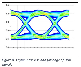 AMI also assumes that rise and fall edges are symmetrical in the signal. While this may be a valid assumption for differential I/O, it is typically not the case for single-ended I/O, where the pullup and pulldown slew rates are usually noticeably different. As a result of asymmetric edges, the single-ended eye is asymmetrical vertically, and its crossing level is shifted either upward or downward from the center voltage of the eye, impacting both voltage and timing margins. To capture these effects, advanced AMI simulation algorithms are developed to take into account the difference between rise and fall waveforms.
Fig. 8 shows a DQ eye at the Rx pad generated by an AMI simulation. In the plot, the rise and fall edges are asymmetric as is typical for a single-ended signal, and the crossing level is shifted upward from the center voltage of the eye due to the asymmetric nature. Note that Fig. 8 also shows the DC offset of the single-ended DQ signal.
New forwarded clocking solution
In the AMI specification, it is assumed that every Rx has its own CDR circuitry to recover the clock from the data, and the AMI_GetWave function has only one input waveform, which is the data signal. However, DDR channels employ the so-called clock forwarding architecture, where, instead of using an internal CDR, the DQ Rx uses a data strobe signal (DQS) as the forwarded clock to clock the DQ Rx DFE slicer and data sampling. Practically, the DQ Rx device has two input signals, one is data, and the other is clock. To enable modeling of clock forwarding, a new Rx AMI_GetWave API, originally known as GetWave2, is established in IBIS BIRD 204 and approved for a future release of IBIS specification. The API defines two input waveforms for data and clock signals respectively. The DQ Rx clocking behavior can be physically modeled in the new AMI_GetWave function.
Phase Interpolator in forwarded clocking
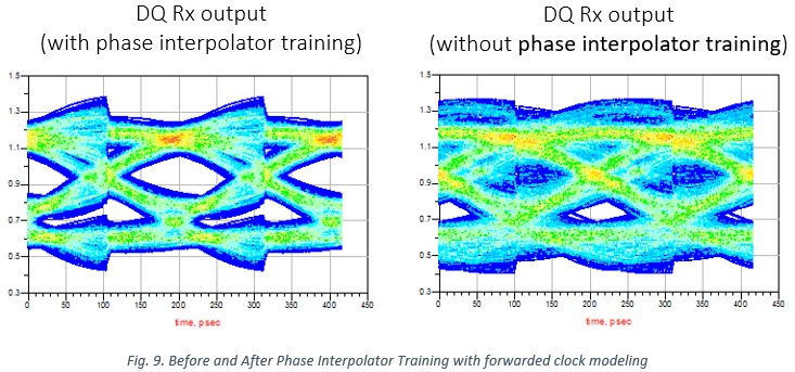
Besides clock forwarding, another key clocking functionality that can be modeled using the new AMI_GetWave API is the phase interpolator in the controller DQ Rx. During READ cycles, the controller DQ Rx PI applies a 90deg. phase shift to the forwarded DQS signal and mixes it with the original one. The resulting signal is a delayed DQS signal, and the delay value depends on the mixing weights. During system training, the controller tunes the weights and, therefore, the delay to adjust the DQ-DQS skew for optimal DQ Rx DFE clocking in READ operations. Fig. 9 shows a READ cycle controller DQ post-DFE eye with and without PI training modeled by the new AMI_GetWave API. The training aligns DFE switching with data bit edges to help open the eye.
Jitter tracking with forwarded clocking
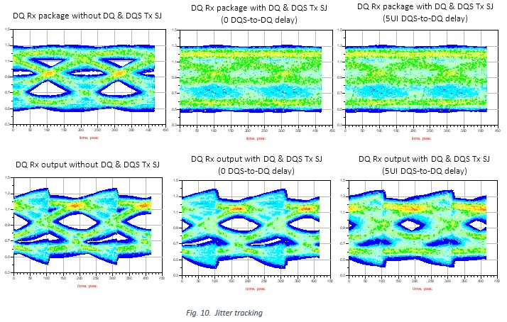
One advantage of the clock forwarding architecture is jitter tracking. Because the DQS signal is used to clock the DQ Rx, when the DQ is sampled, correlated jitter between DQ and DQS are cancelled. On the other hand, the DDR5 spec allows certain amount of electrical path mis-match between DQ and DQS Rx. The mis-match reduces the DQ-DQS jitter correlation and adversely impacts the effectiveness of jitter tracking and DFE. With the new AMI_GetWave API, both jitter tracking and the effect of unmatched Rx can be captured naturally in AMI simulations. Fig. 10 shows simulated eyes of a DQ signal at the Rx package pin and at the Rx DFE output.
Without Tx jitter, the eye is almost closed by ISI at the package but opened by the DFE at the Rx output. When SJ is injected to DQ and DQS Tx, the eye is completely closed at the package. In the case of matched Rx (with zero DQS-to-DQ delay) DQ and DQS jitters are correlated and tracked by DQ sampling times, leaving the DQ post-DFE eye almost unchanged from that without Tx SJ. In the case of unmatched Rx (with a 5UI DQS-to-DQ delay) the DQ-DQS jitter correlation is reduced, and the jitter tracking becomes less effective, leading to a worsen DQ post-DFE eye.
Conclusion
In this article, we reviewed the basics of IBIS and IBIS-AMI models. IBIS/IBIS-AMI models are very effective vehicles for chip vendors to communicate and share their intellectual propertiy with customers without harming their design secrets. Also, from the system vendor’s point of view, it is the fastest and easiest way to evaluate and validate their designs instead of going through multiple board spins. That is why IBIS/IBIS-AMI models have been very popular in high-speed digital designs and became the market standard for DDR and SERDES applications.
Due to the ever increasing speed-grade of memory systems, it is necessary to apply equalizations, which creates severe burdens for memory system design engineers. Fortunately, the challenges have been overcome by an IBIS-AMI solution for single-ended signals and the introduction of a forwarded clocking solution in BIRD 204. We anticipate new challenges when the next generation of memory systems comes, such as (LP)DDR6 or GDDR7, but we can count on new solutions coming out to help design engineers.
References
[1] IBIS specification version 7.0